


Contents
Modern electronic designs such as mobiles, laptops, cloud computing, and networking demand very high performance. Apart from processor speed/performance, memories play a very critical role in overall system performance. Double Data Rate (DDR) memories have been a common choice of designers in all complex devices due to their low latency, bigger storage size, and low power consumption.
Introduction to memory system
Memories are the data storage devices in electronic products. They store the processed information/data and make it available to the controller whenever requested. At a high level, memories are categorized into primary memory and secondary memory.
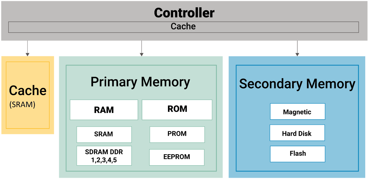
Primary memory is further categorized into Random Access Memory (RAM) and Read-Only Memory (ROM). RAM is a volatile memory and data will be lost after the power is switched off. ROM memory retains the data even after power is turned off. As the VLSI technology advanced, memory construction, memory chip density, size, speed, and communication interface have been improved to a great extent.
Difference between SRAM and SDRAM
RAM is further categorized into SRAM and SDRAM. SRAM is Static RAM and SDRAM is Synchronous Dynamic RAM. The architectural difference between the two is that DRAM uses 1 transistor and 1 capacitor per memory bit, whereas SRAM uses 1 flip-flop (~ 6 transistors per flip-flop) to form one bit. The SDRAMs are slightly slower due to higher access time compared to SRAMs. As the size of a capacitor/transistor is smaller than that of a flip-flop, the memory density of SDRAM is higher compared to SRAM. SDRAM is dynamic storage since the capacitors tend to discharge over time, and unless they are refreshed periodically SDRAM will not retain the stored data.
SRAM has been a default choice for cache memory as they are extremely fast and have very low access time. They reside internally in the processor or can be interfaced externally. The cache acts as a buffer between external RAM and the processor. This memory stores the frequently used data/instructions and makes them immediately available to the processor whenever requested. In general, cache memory reduces the average time to access data from the Main memory.
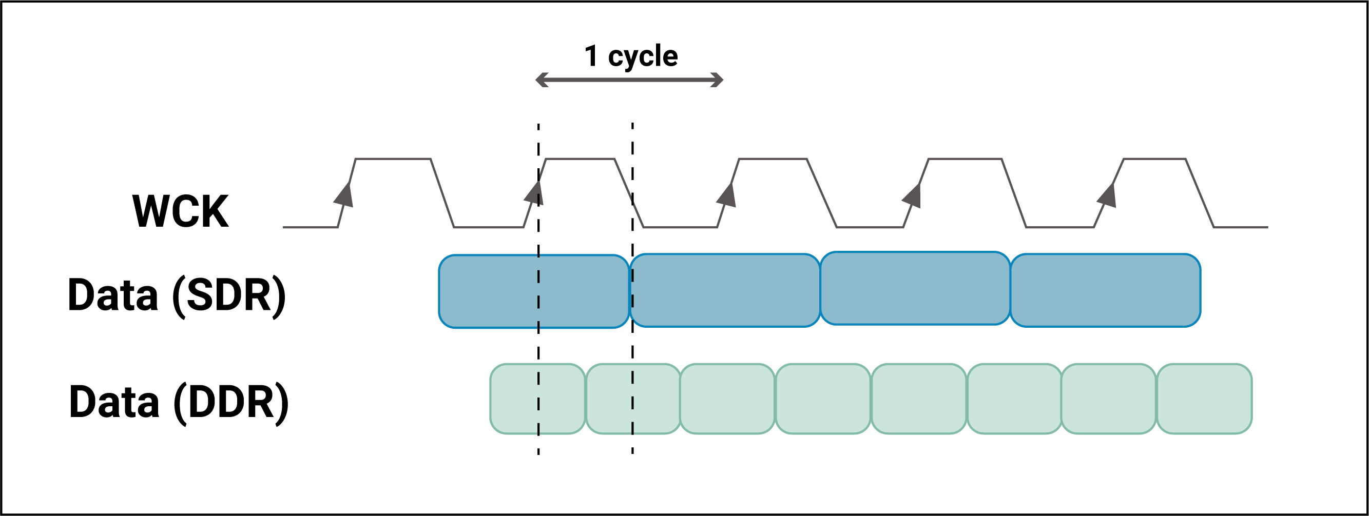
As stated earlier, SDRAM stands for synchronous dynamic RAM where the I/O, internal clock and bus clock are synchronous. For instance, the PC133 I/O, internal clock and bus clock are all 133MHz. Single Data Rate signifies that SDR SDRAM can only read/write one time per clock cycle. The SDR SDRAM needs to wait for the completion of the previous command to be able to do another read/write operation.
What are the different types of DDR RAMs?
The demand for higher data rates and larger data densities lead to the evolution of SDR into the DDR concept. The demand for higher data rates and larger data densities lead to the evolution of SDR into the DDR. In the DDR SDRAM, the data is clocked at both edges – positive as well as negative edge – which results in doubling the data rate. In this way, DDR achieves greater bandwidth compared to SDR SDRAM; it doubles the transfer rate without increasing the frequency of the clock.

Over the last few decades, many memory improvements have occurred in DDR technology. The DDR has become extremely popular in the market and is used extensively in notebooks, laptops, servers, and embedded computing systems. The DDR offers many enhancements such as increased speed of operation, improved storage densities, reduced power consumption, and adds error detection functions such as CRC, reduced SSN noise by implementing the bit inversion concept. In the following section, we will discuss the evolution of DDR memories and their benefits.
First-generation – DDR SDRAM
The first generation of DDR memory had a prefetch buffer of 2-bit, which is twice that of SDR SDRAM. The internal clock speed of 133 ~ 200MHz gave the transfer rate of DDR1 as 266 to 400 MT/s (Million Transfer Per Second). The DDR1 ICs were released in the market in the year 1998.
Second-generation – DDR2 SDRAM
DDR2 operates with an external data bus twice as fast as DDR1 SDRAM. This is achieved by the improved bus signal. The prefetch buffer of DDR2 is 4-bit which is double that of DDR SDRAM. DDR2 memory has the same internal clock speed (133 ~ 200 MHz) as the DDR memory. However, the DDR2 memory has improved the transfer rate (533 ~ 800 MT/s) and the I/O bus signal. DDR2-533 and DDR2-800 memory types were released in the market in the year 2003.
Third-generation – DDR3 SDRAM
DDR3 operates at double the speed of DDR2. This is achieved by further improvements in the bus signal. DDR3’s prefetch buffer width is 8-bit which is double of DDR2. The transfer rate of DDR3 memory is 800 ~ 1600 MT/s. DDR3 operates at a low voltage of 1.5V compared with DDR2’s 1.8V which results in 40% less power consumption. The DDR3 has two added functions namely – ASR (Automatic Self-Refresh) and SRT (Self-Refresh Temperature).
The DDR3 ICs were released in the market in the year 2007.
Fourth-generation – DDR4 SDRAM
DDR4 operates with double the speed of DDR3. DDR4 operates on low operating voltage (1.2V) and higher transfer rates. The transfer rate of DDR4 is 2133 ~ 3200MT/s. DDR4 adds four new bank groups technology. Each bank group has the feature of a single-handed operation. The DDR4 can process 4 data within a clock cycle, so DDR4’s efficiency is better than DDR3. DDR4 has some additional functions such as DBI (Data Bus Inversion), CRC (Cyclic Redundancy Check) on data bus, and Command/Address parity. These functions can enhance DDR4 memory’s signal integrity and improve the stability of data transmission/access. Independent programming of individual DRAMs on a DIMM allows better control of on-die termination.
The DDR4 ICs were released in the market in the year 2014.
Fifth-generation – DDR5 SDRAM
Next-gen memory DDR5 operates at double the speed of DDR4. The transfer rate of DDR5 is 3200 ~ 6400 MT/s.The DDR5 specification was released in November 2018, and ICs are expected to be on the market by 2022.
Enhancements in DDR5 Vs DDR4
We will now discuss the most significant changes in DDR5 versus DDR4.
Speed improvements:
- Improved clock speed (1.6GHz to 3.2GHz)
- Improved data speed (3.2Gbps to 6.4 Gbps)
- Inclusion of new features such as Decision Feedback Equalization (DFE)
Lower voltage level:
The operating voltage VDD is changed from 1.2V to 1.1V, which reduces power consumption. On the other side, lower VDD means a smaller margin for noise immunity.
Introduction of power architecture for DDR5:
With the addition of DDR5 DIMMs, power management moves from the motherboard to the DIMM itself. DDR5 DIMMs have 12V power management IC which allows better granularity of system power loading and helps with signal integrity and noise issues.

Controlled Impedance Design Guide
6 Chapters - 56 Pages - 60 Minute ReadWhat's Inside:
- Understanding why controlled impedance is necessary
- Stack-up design guidelines
- How to design for impedance
- Common mistakes to avoid
Download Now
Improvement in channel architecture DDR5:
DDR4 DIMMs have a 72-bit bus comprising 64 data bits plus eight ECC bits (Error Correcting Code). In DDR5, each DIMM will have two 40-bit channels(32 data bits and 8 ECC bits). While the data width is the same (64-bits total) having two smaller independent channels improves DDR memory access efficiency. The benefit of this is higher MT/s is amplified by greater efficiency.
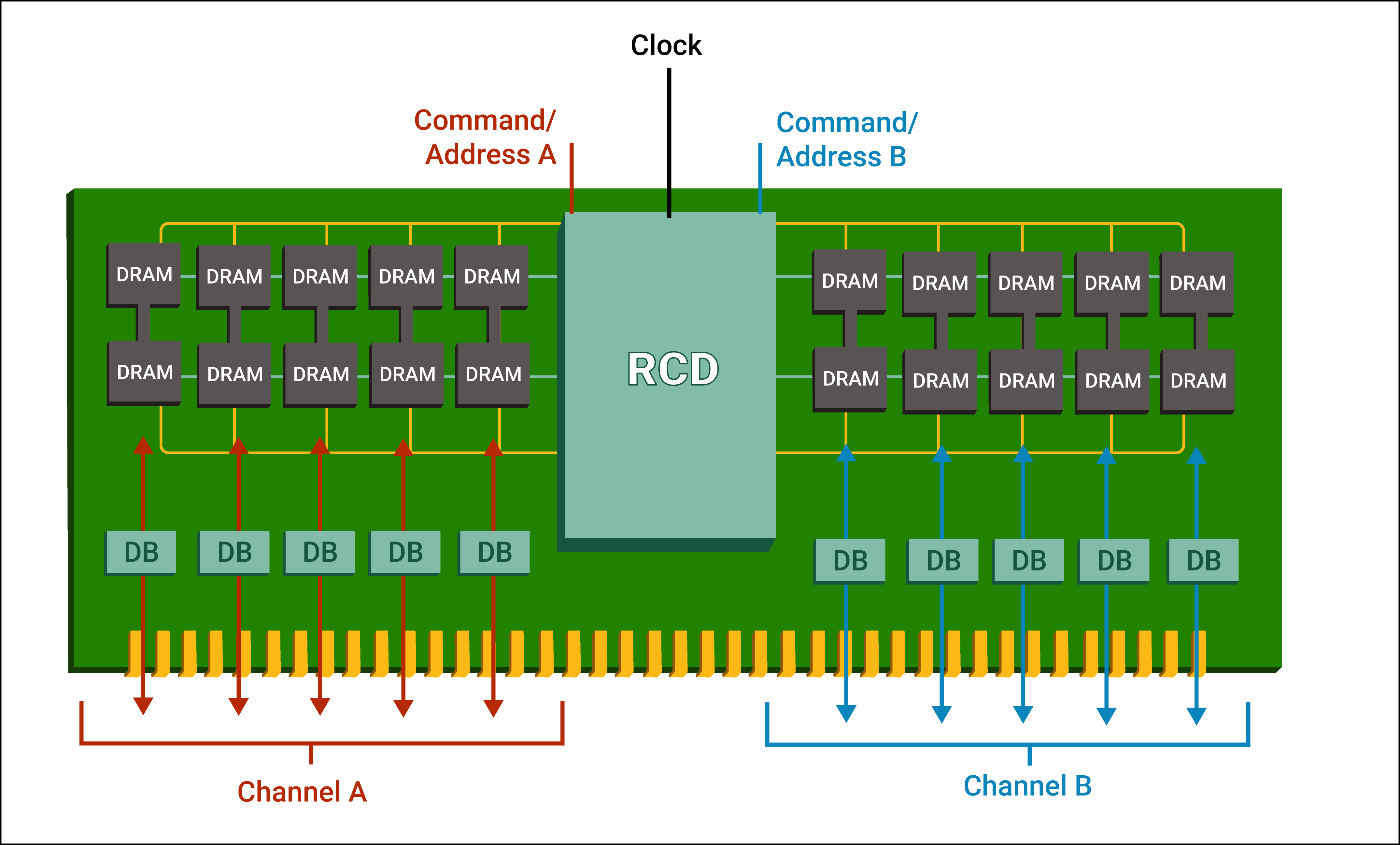
In DDR4, the RCD Registered Clock Driver (RCD) provides two output clocks per side. The RCD in DDR5 provides 4 output clocks per side, providing each lane an independent clock. This improves signal integrity and helps us to address the lower noise margin issue that occurs due to reducing the VDD.
Enhanced burst length to 16 in DDR5:
The DDR4 burst length is eight whereas, for DDR5 the burst length will be extended to eight and sixteen to increase burst payload. Burst length of 16 (BL16) enables a single burst to access 64 bytes of data. This results in a significant improvement in concurrency and with two channels, greater memory efficiency.
Supports higher capacity DRAM:
DDR5 buffer chip DIMMs enable the system designers to use densities of up to 64 Gb DRAMs in a single-die package. DDR4 provides 16 Gb DRAM in a single-die package.
In the following table, we have compared some of the critical features of various generation DDR RAMs for a better understanding.
| Features/Option | DDR2 | DDR3 | DDR4 | DDR5 |
|---|---|---|---|---|
| Voltage (Core, I/O) | 1.8V | 1.5V | 1.2V | 1.1V |
| Chip Storage Densities | 256Mb-4Gb | 512Mb-8Gb | 2Gb-16Gb | 8Gb-64Gb |
| Internal Banks | 4 -> 8 | 8 | 16 | NIL |
| Bank Groups | 0 | 0 | 4 | |
| Page Size x4/x8/16 | 1KB/1KB/2KB | 1KB/1KB/2KB | 512B/1KB/2KB | |
| Internal Rate | 100 to 166 MHz | 133 to 200 MHz | 133 to 200 MHz | 133 to 200 MHz |
| Clock DLL -enabled | 125-400Mhz | 300-800Mhz | 625 Mhz-1.6Ghz | |
| Data rate Mb/s | 400 / 553 / 667 / 800 / 1066 | 800 / 1066 / 1333 / 1600 / 1866 / 2133 | 1600 / 1866 / 2133 / 2400 / 2667 / 3200 | 3200 / 6400 |
| Prefetch(n=bits) | 4n(2-clk) | 8n(4-clk) | 8n(4-clk) | 16n |
| Burst Length | BC4/BL8 | BC4/BL8 | BC4/BL8 | BL16/BL32 |
| Data Strobe | Single/ Differential | Differential | Differential | Differential |
| Clock | Single | Differential | Differential | Differential |
| DQ Bus voltage | SSTL1.8V | SSTL1.5V | POD1.2 | 1.1V |
| Rtt values | 150, 75, 50 Ohms | 120,60,40,30,20 Ohms | 240,120,80,60,48,40,34 Ohms |
Memory data transfer speed
The speed of the DDR memory data transfer determines how fast programs will execute. The importance of transfer rate is clearly realized when you are running multiple software applications simultaneously or an imaging application. The memory transfer rate is determined by three factors such as memory bus clock rate, the type of transfer process, and the number of bits transferred.
| Names | Memory clock | I/O bus clock | Pre-fetch n = data bits | Data Transfer rate = 2 * I/O clock | Theoretical bandwidth = data Trnsfr * 8 Byte |
|---|---|---|---|---|---|
| DDR1-200, PC-1600 | 100 MHz | 100 MHz | 2n | 200 MT/s | 1.6 GB/s |
| DDR1-400, PC-3200 | 200 MHz | 200 MHz | 2n | 400 MT/s | 3.2 GB/s |
| DDR2-800, PC2-6400 | 200 MHz | 400 MHz | 4n | 800 MT/s | 6.4 GB/s |
| DDR3-1600, PC3-12800 | 200 MHz | 800 MHz | 8n | 1600 MT/s | 12.8 GB/s |
| DDR4-2400, PC4-19200 | 300 MHz | 1200 MHz | 8n | 2400 MT/s | 19.2 GB/s |
| DDR4-3200, PC4-25600 | 400 MHz | 1600 MHz | 8n | 3200 MT/s | 25.6 GB/s |
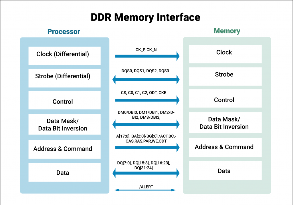
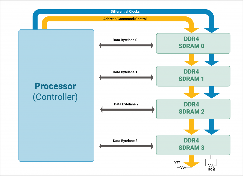
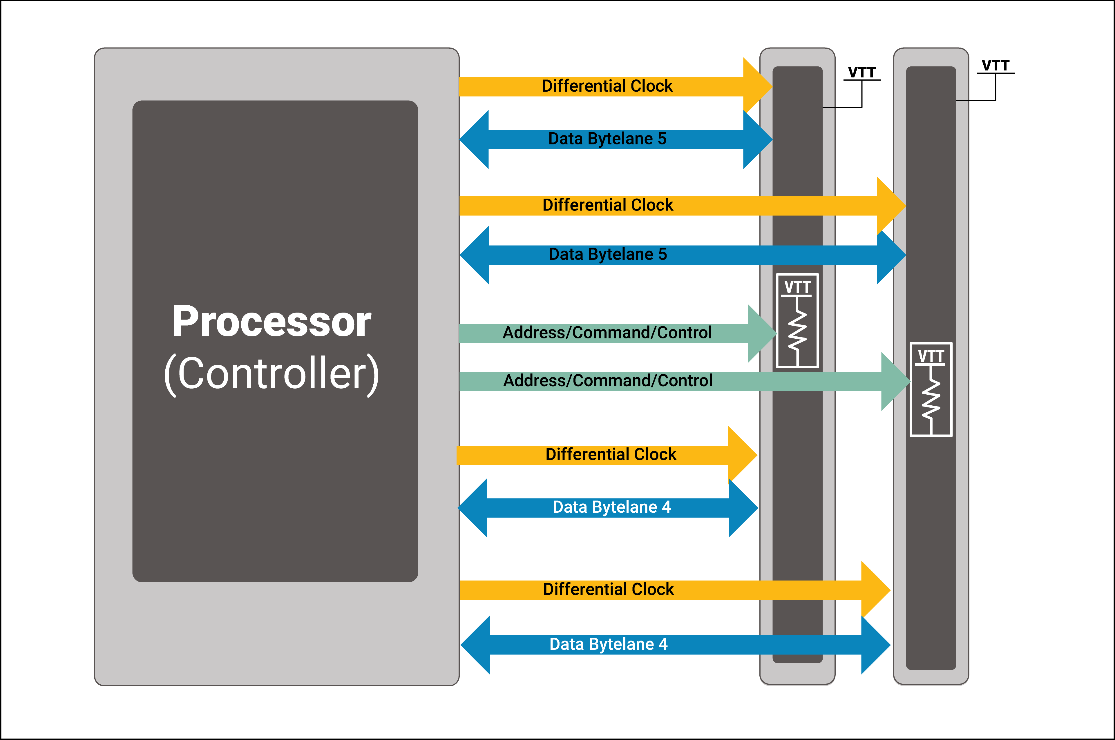
Brief working operation of DDR4
The interface between memory and the processor for DDR4 standard is shown in the following figure. This interface consists of group signals which include data, address, clock, and control signals.

Interfacing signals
The below table lists some of the basic and important signals used in data transfer between processor and SDRAM memory.
| Symbol | Type | Function |
|---|---|---|
| CS_n (Differential) | Input | Chip select is active low signal, this signal enables the memory IC for read/write operation |
| CKE | Input | Clock Enable. HIGH enables the internal clock signals device input buffers and output drivers. |
| CK_t/CK_c | Input | Clock is a differential signal. All address and control signals are sampled at the crossing of posedge and negedge of clock. |
| DQ(single)/ DQS_t/DQS_c (Differential) | In/out | Data Bus is single-ended signal whereas Data Strobe is differential signals. Data is read or written in memory with respect to strobe signal. It acts as data valid flag. |
| RAS_n/A16; CAS_n/A15; WE_n/A14 | Input | These are dual function inputs. When ACT_n and CS_n signals are LOW, these are interpreted as Row Address Bits. When ACT_n is HIGH, these are interpreted as command pins to indicate READ, WRITE or other commands. |
| ACT_n | Input | Activate command input, when this signal is low data on RAS/CAS/WE acts as a command |
| BG0-1 BA0-1 | Input | Bank Group, Bank Address |
| DBI[0-n] | In/out | Data bit inversion |
| A0-16 | Input | Address inputs |
Data Bus configuration
DDR memories are available with data bus widths such as DQ [0:3], DQ [0:7], and DQ [8:15]. In the case of DIMM, the total maximum data bus width is either 32 bits or 64 bits depending upon the processor. In the DDR4 version, additional 8 bits are allocated for error control hence total bus width becomes 40 bits/72 bits.
Data Bus Inversion (DBI) function:
DDR4 deploys Data Bus Inversion to mitigate simultaneously switching noise, due to which power noise improvement and intermittent reduction in IO power are observed. DBI# is an active low and bidirectional signal. During the write operation, If DBI# is sampled low, DRAM inverts the write data received on the DQ inputs. If DBI# is high, DRAM leaves the data received on the DQ inputs non-inverted. During the read operation, the read data on its DQ outputs are inverted by DRAM. The DBI# pin is driven low when the number of ‘0’ data bits within a given byte lane is greater than 4; else the read data will not be inverted by the DRAM and drives the DBI# pin HIGH.
Write leveling for better DQ timing
In DDR4, memories are routed in Fly-by topology rather than Tree-topology; this was done especially to reduce the reflection caused during high-speed data transfer. The clock (and address) signals in Fly-By routing begin at the controller and establish the main channel to all the DRAMs. The DRAMs are connected to the main path by means of a very short stub from the main routed signal. However, this creates a problem with respect to the clock-to-DQS requirement at the DRAM. The DRAM closest to the controller will receive the clock and address signals before the last DRAM.
Mismatch in length and signals of address/clock paths in memories can create issues during the read cycle hence “Write leveling” solutions are implemented in DDR4. These solutions enable the controllers to automatically detect the flight-time difference between the clock signals of different DRAMs. Later, it delays the data lanes appropriately so that they reach the DRAMs as the clock/address signals reach the DRAMs. This process of detecting the required delays is called “training.” It is also possible to delay each DQ bit within a lane with regards to its strobe to perfectly center the strobe around the DQ signal.
READ operation with a burst length of 8 (BL8)
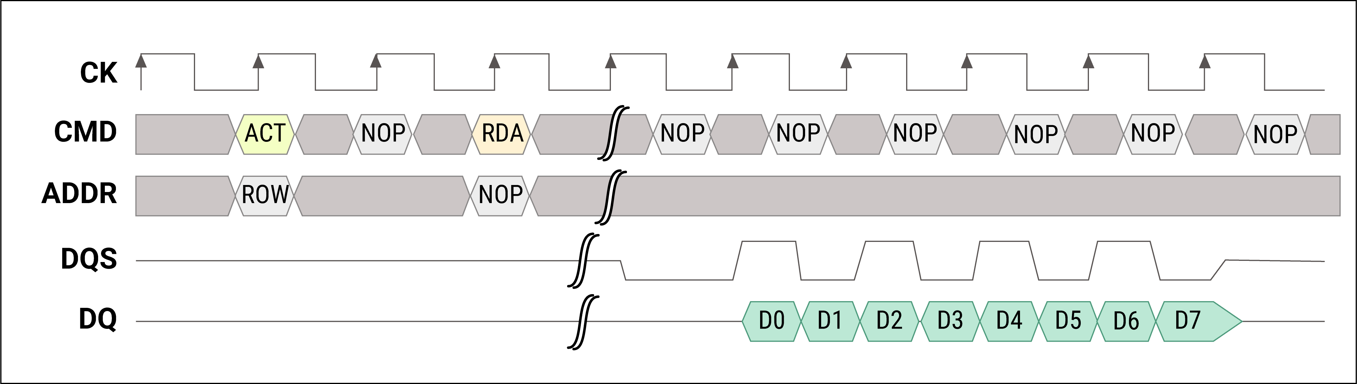
- In the beginning, the processor sends an ACT command, the value on the address bus at this time indicates the row address. The ACT command is clocked at the first posedge of the clock along with row address. Remember, command lines are multiplexed with address bus.
- The next step is that the processor sends RDA (Read with Auto-Precharge). The value on the address bus at this time indicates the column address. At the third clock edge, this is latched into the memory.
- Next, the DQS signal clock is the output from the memory. During the read operation both the edges are aligned to the data.
- Succeeding this, the processor sends RDA command which is interpreted by DRAM to automatically PRECHARGE the bank after the read is complete.
Write operation with a burst length of 8 (BL8)
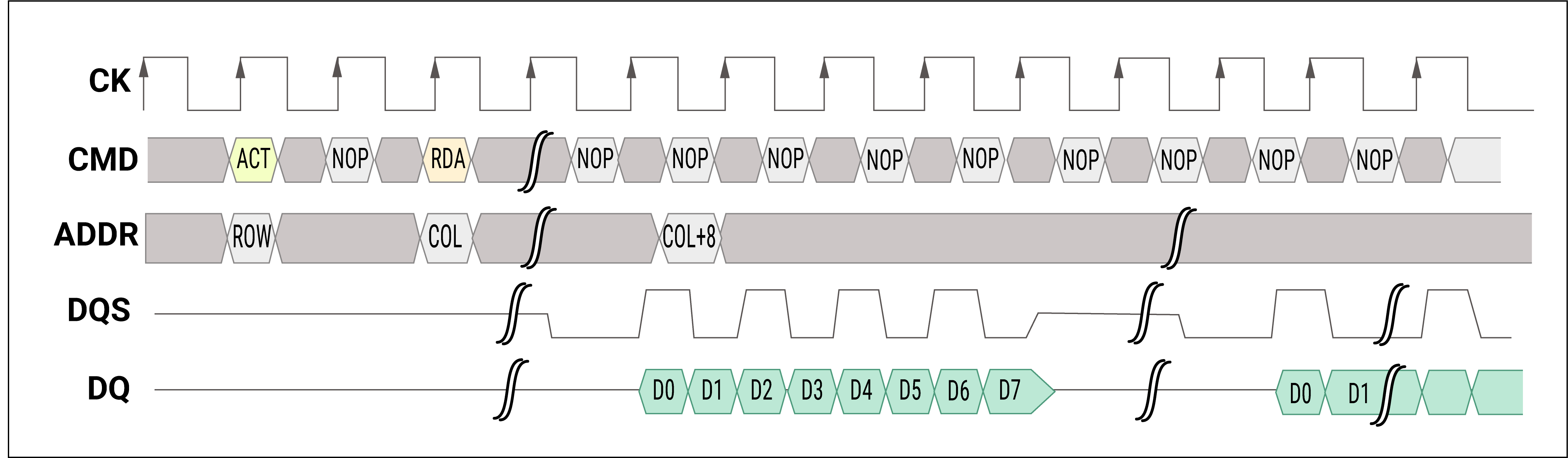
- In the beginning, the processor sends an ACT command, the value on the address bus at this time indicates the row address. The ACT command is clocked at the first posedge of the clock along with the row address.
- The next step is that the processor sends 2 WRITE commands. The first one indicates the COL address and the second one refers to COL+8. At the third clock edge, this is latched into the memory.
- The second write operation does not need an ACT command. This is because the row we intend to write to is already active in the Sense Amps.
- Next, the strobe DQS signal clock is the output from the processor during the write operation along with data at both edges of the strobe signal.
- Also, note that the first command is a plain WR, so this leaves the row active. The second command is a WRA which deactivates the row after the write completes.
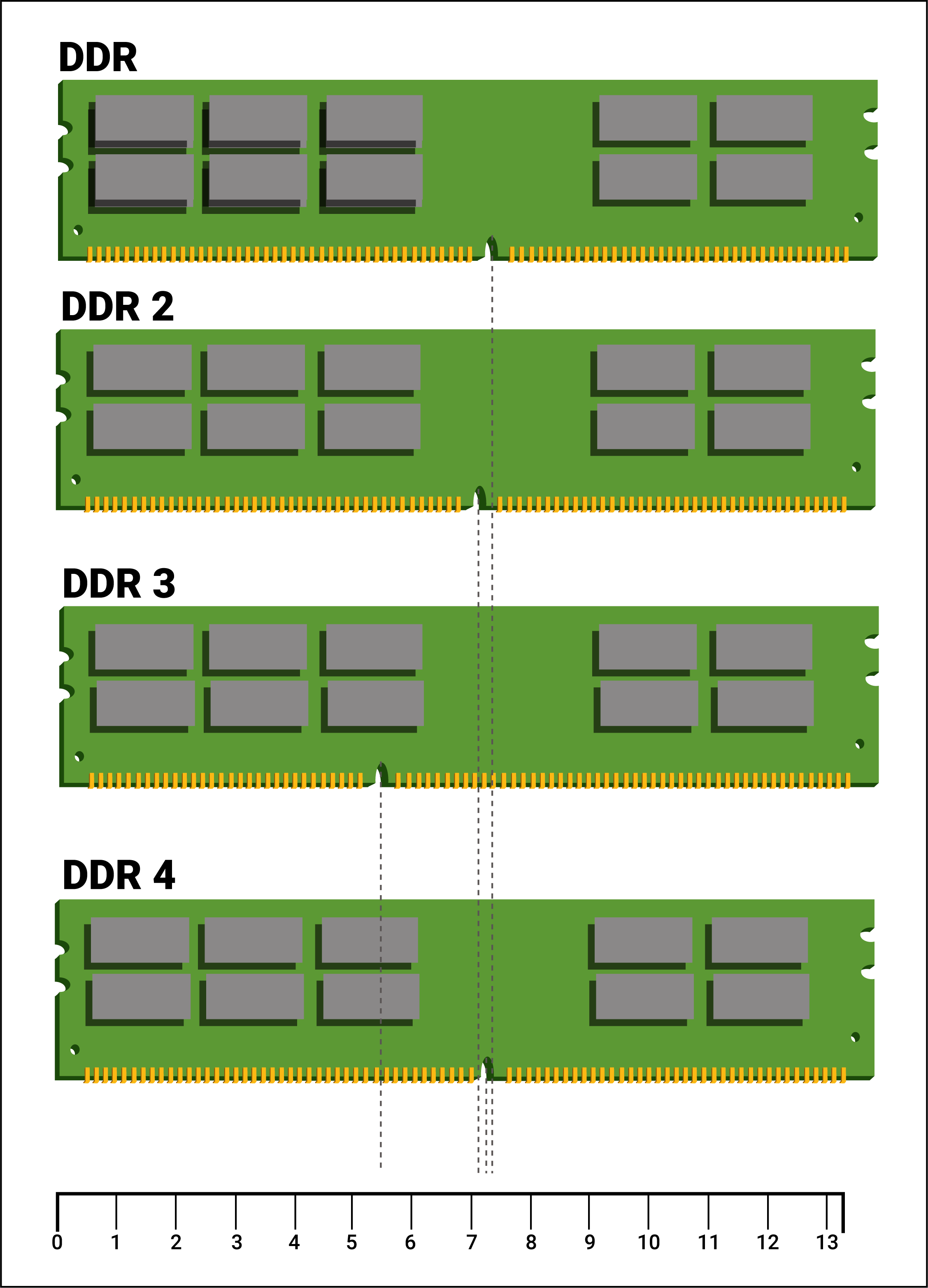
DDR modules
In order to increase the overall memory size in terms of capacity and bandwidth, DDR memories are combined on a single PCB which is called a module. Each DIMM can have multiple chips numbering from 4-16 ICs placed on both sides of a PCB to create 2 GB, 4 GB, 8 GB, 16 GB, and 32 GB memory modules. For example, the 64-bit data bus for DIMM requires eight numbers of 8-bit chips, addressed in parallel. A set of DRAM chips with the common address lines are called a memory rank. All the ranks will be connected to the same memory bus. The chip select signal can be used to issue commands to a specific rank.
Based on the size they have three form factors, they are DIMM (Dual In-line Memory Module), SODIMM, and MICRODIMM.
| Type of DIMM | DDR | Pin count |
|---|---|---|
| DIMM SODIMM MICRODIMM | DDR1 | 184 200 172 |
| DIMM SODIMM MICRODIMM | DDR2 | 240 200 214 |
| DIMM SODIMM MICRODIMM | DDR3 | 240 204 214 |
| DIMM SODIMM MICRODIMM | DDR4 | 288 260 |
All DDR memory modules are mutually incompatible. The DDR2/3/4 DIMMs can only be used on their respective DDR2/3/4 sockets, with the notches differently located. The power supply for each variant also changes: for DDR1 DIMMs, it’s 2.5V; DDR2, 1.8V; DDR3, 1.5V; and DDR4, 1.2V. Hence the user needs to take precautions to check the DDR memory version before ordering a memory module for their computer/device.
Applications of DDR memories and selection parameters
DDR Memories are used in the following devices/systems:
- Computers, laptops, supercomputers, servers, etc.
- Mobile devices, tablets
- Gaming devices
Selection parameters:
- Verify your processor memory controller interface and support to DDR4 interface
- Type of memory required in the design
- Memory size
- Clock frequency requirements
- Interfacing speed
- The rise time of the clock and data bus
- Access time
- Write cycle time
- Setup and hold time values command, address, control
- Core and IO voltages requirement
- VIO/VIH and VOL/VOH of signals
- Type of package
Packages:
Widely used packages for higher-size memories are BGA, FBBGA, WFBGA, TFBGA, QFPN etc.
IC manufacturers:
Micron Technology, ISSI, Winbond, Cypress, STMicroelectronics, Alliance Memory, etc.
Module manufacturers:
Cypress, Kingmax, Micron, Electronics, Centon Electronics, etc.
Key challenges in PCB routing for DDR memories
High-speed PCB design typically needs to meet certain timing requirements in order to perform correctly. However, in the case of DDR4 RAM, this timing is tightened due to higher data rates. The design will fail if timings are not met, resulting in a higher bit error rate/data corruption. The designers are expected to carry out board simulations for signal integrity at every step.
In the case of DDR memories, because of data transfer at both edges of the clock/strobe and high clock rate 1.6GHz, the setup and hold times are shorter and therefore timings delays play a significant role. The methods to achieve the requirements are discussed below.
The major challenges in routing DDR4 SDRAM interface with Gigabit transmission include:
- The method to maximize the timing margin of the data transmission, controlling the accurate Setup/Hold time
- The routing topology and appropriate termination scheme for nets with multiple receivers
- Routing technique to minimize crosstalk
- Method to mitigate the impedance discontinuity due to imperfect vias.
- Clean supply voltages
- Trace length matching
Need help with high-speed routing DDR4 or DDR5 memory designs? Check out our PCB design support.
You can book a meeting with our experts or call us at +1 (800) 763-7503.

PCB design rules for DDR memories
Proper setup time and hold time
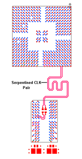
Adjusting the trace length of the clock with respect to data lines and control signals so as to comply with the setup and hold times of memory IC. The clock signal can be delayed by routing it in a serpentine fashion.
Clean and stable reference voltages
DDR4 requires extremely clean and stable voltages since it runs on low voltages (1.2V). The supply voltage is delivered through the power plane to the memory and to the termination resistors on the same side of the board, thus eliminating the impedance due to vias. Capacitors should also be evenly placed, which creates a consistent, clean bypassed reference. The following pictures display the placement of the capacitors in processor/FPGAs.
Placement of capacitors in Processor/FPGA
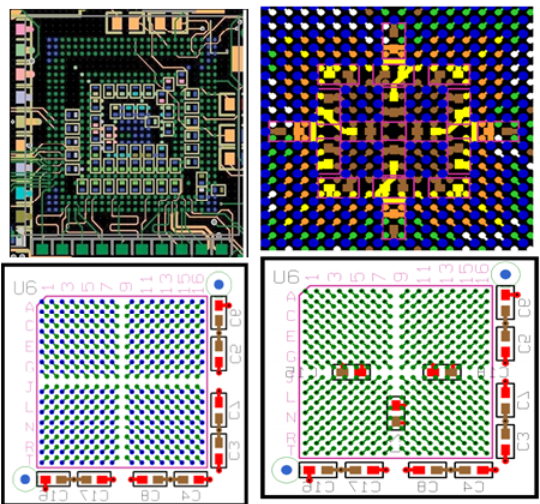
Placement of capacitors in DDR
Decap and bypass capacitors placements
- The fanout scheme creates a four-quadrant structure that facilitates the placement of decoupling and bulk capacitors on the bottom sides of the PCB.
- Usually 0210 or customized 0402 package capacitors should be mounted as close as possible to the power vias. The distance between them should be less than 50 mils.
- An additional bulk capacitor can be placed near the edge of the BGA via array.
- Placing the decoupling capacitors close to the power ball is critical to minimize the inductance. This also ensures high-speed transient current demand by the processor.
- Choosing a proper via size helps the designers in preserving adequate routing space.
- The recommended geometry for the via pad is: pad size is 18 mils and drill 8 mils.
- Place the largest capacitance in the smallest packages that budget and the manufacturing can support. For high-speed bypassing, select the required capacitance with the smallest packages (For example, 0.22uF and package 0201)
- Minimize trace length (inductance) to small caps.
- Series inductance cancels out capacitance.
- Tie caps to GND plane directly with a via.
DDR placement and routing rules
- The ultimate purpose of the placement is to limit the maximum trace lengths and allow proper routing space.
- The placements do not restrict the side of the PCB on which the device are mounted.
- Fly-by topology is preferred over the tree topology based on the study conducted by the researchers. It has shown improvement in the data eye diagram. The advantage of fly-by topology is that it supports higher-frequency operation, reduces the quantity and length of the stubs, and consequently improves the signal integrity and timing on heavily loaded signals.
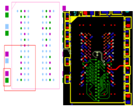
Routing traces for on-board DDR and DIMM is shown below.
Bus topologies—On-board two-UDIMM
Signal grouping
Before routing the DDR signals we have to group the signal first in a specific way,
- Group should include 8 bits of data, data strobes and mask data/Data inversion which makes 11 signals. For example, signals are as follows:
-
- BYTELANE0 DQ [7:0], DM0/DBI0, DQS_P0, DQS_N0
- BYTELANE1 DQ [15:8], DM1/DBI1, DQS_P1, DQS_N1
-
- The address can be grouped separately including control, commands and related clock signals.
- Once data grouping is done and it should be routed as short as possible to the processor.
- The address, command, and control signals operate at half the bandwidth of the data, so they are expected to be longer.
Signal routing
- Data lines are routed as short as possible from the processor.
- Address lines, command, control lines are operating at half the bandwidth of the data, so they expected to be longer.
- The data byte and control line from the same channel/group should be routed on the same layer.
- Address/command/control/differential clock should be routed on the same layer, but if space issue arises, they can be routed on the different layers also.
- Address/command/control/differential clocks are route topology
- T-Topology
- Daisy-chain(Fly-by) Topology
- Route from controller starting with chip 0 thru chip n routing in order by byte lane numbers. Chip 0 is the lower data bit (Bytelane0)/chip. ‘n’ represents the upper data bit (Bytelane3).
- Advantages of fly-by topology:
- Supports high-frequency operation
- Reduces the quantity and length of the stubs consequently improves the signal integrity and timing on heavily loaded signals.
- Reduces simultaneous switching noise (SSN) by causing flight-time skew between address and the point to point topology signals of the data group.
- Fly-by topology has very short stubs. This eliminates reflections.
- In T-topology, the trace stub is lengthened with an increase in the number of memory device loads.
- In T-topology, the clock traces need to be routed with a prolonged delay than the strobe traces per byte lane.
- In most of the cases DDR2 and its previous classes follow the T-topology routing.
- DDR3 and the next generations all of its classes follow Fly-by topology routing.
To know more about PCB routing read our article 11 Best High-Speed PCB Routing Practices.
Trace length matching
The length matching is done in groups. Common length matching route groups are:
- Clock-to-Address/Command Group
- Clock-to-Strobes Group
- Strobe-to-Data Group
Match the lengths of signals using a serpentine path. Follow routing guidelines for data byte lanes as per the manufacturing datasheet. The maximum skew among all the signals shall be less than +/-2.5% of the clock period driven by the memory controller. The clock traces should be slightly longer than data/strobe/control lines so that clock arrives at the destination later than the data/strobe/control.
For example, if the normal FR4 material with a dielectric constant of 4 is used on the PCB, at a different clock rate of 1.2GHz (i.e., 833ps clock period), the maximum skew shall be +/-125mil(25psec) among all the signals.
Relative propagation delay
- 1 –5mils between all members inside of byte lane
Address/command/control
- 100 –200mils between controller to first memory IC
- Clock to address/command +/- 25psec (125 mills)
- 10 –20mils between memory ICs
Propagation delay
- 1500 –1750mils from controller to first memory IC.
- 650 –750mils between memory ICs.
Differential phase tolerance
- 1 –5mils for all data strobe and clock differential pairs
Data bus termination
- Series resistor termination can be used when point-to-point connection is in 2” to 2.5” range. Resistors to be located at the center of the transmission line.
- Use DRAM termination with direct connect using on-die termination (ODT) to improve the signal quality and cheaper price.
Clock termination
- 100 ohms differential terminator at the last SDRAM device in the chain is placed. This is 100 Ohms differential signal.
Characteristics impedance of traces
For single-ended traces such as data lines characteristics impedance is 50Ω and differential traces such as Clock and Strobe it is 100Ω.
- Single-ended impedance = 50Ω
- Smaller trace widths (5–6 mils) can be used.
- Spacing between like signals should extend to 3x (for 5 mils) or 2.5x (for 6 mils), respectively.
Crosstalk
The crosstalk issue becomes more severe, especially in HDI PCBs, when traces run at high frequency and high edge rate. In order to minimize the coupling effect from the aggressor to the victim the spacing between two adjacent signal traces shall be at least 2 times and typically 3 times the trace width. However, the large trace spacing is tough to be implemented on the PCB due to space constraints.
Board simulation
To obtain best performance, a layout designer needs to carry out board simulation for signal integrity and cross talk. Designers should ensure that optimal termination values, signal topology, and trace lengths are determined through simulation for each signal group in the memory implementation. To learn how to get rid of cross talk issues in HDI PCBs, read our article How to Avoid Crosstalk in HDI Substrate?
PCB design guidelines
- Plan the board stack-up.
- Plan the trace width and spacing between traces.
- Plan the component placement carefully, such as memory IC’s in daisy chain topology, and place termination resistor, filter capacitors etc as per the guidelines
- Plan the ground and power plane as per the digital and analog components.
- Measure the lengths of Nets/signals of byte lanes.
- Import the right IBIS (Input/Output Buffer Information specification) model given by IC manufacturer.
- Place the components and power plane as per plan and route some of the critical single-ended and differential signals first(clock/strobe) and measure the length of the first/last bit of bus for length matching.
- Add delays in lines wherever necessary using additional serpentine traces.
- Measure the via impedance.
- Designers need to work back and forth between layout and simulation while doing the routing.
- Verify compliance with setup/hold times/skew/delays.
- Check crosstalk between the signals.
- No compromise on signal integrity is the key solution to get optimum performance.

High-Speed PCB Design Guide
8 Chapters - 115 Pages - 150 Minute ReadWhat's Inside:
- Explanations of signal integrity issues
- Understanding transmission lines and controlled impedance
- Selection process of high-speed PCB materials
- High-speed layout guidelines
Download Now


