


Contents

On-demand webinar
How Good is My Shield? An Introduction to Transfer Impedance and Shielding Effectiveness
by Karen Burnham
Back drilling is a PCB fabrication technique used to remove the unused portion of a plated through-hole (PTH), known as a via stub.
It helps you minimize signal reflections, resonance, and impedance discontinuities that can degrade signal integrity in high-speed designs.
Circuit board designers working on high-speed digital systems, backplanes, midplanes, and multilayer boards should understand when back drilling is required, how it affects signal integrity, and the design rules needed to ensure manufacturability.
In this article, you’ll learn how back drilling works, when it should be used, and how to implement controlled depth drilling in Altium Designer.
Highlights:
- Use back drilling to minimize signal reflections caused by unused via stubs in high-speed PCB designs.
- Maintain residual stub lengths below 10 mil whenever possible to improve signal integrity.
- Consider alternatives such as microvias, blind vias, and buried vias when they are technically and economically viable.
What is back drilling or controlled depth drilling in PCBs?
Controlled depth drilling (CDD) is a process that removes unused via stubs from plated through-holes using a drill bit slightly larger than the original diameter.
High-speed boards face many challenges in terms of retaining signal integrity, which can be tackled through proper design and manufacturing practices.
A via stub, a non-functional part of a plated hole, causes significant signal integrity issues. It causes reflection of signals from the stub end, and the reflected signal will interfere with the original signal.
To counter this, back drilling is done, where most of the via stub is removed by re-drilling with a slightly larger drill bit.
The back-drilled hole should bring down the stub length to at least 10 mil. If the stubs are greater than 10 mil, then signal reflections will occur.
Why is back drilling required?
Eliminating unused via stubs can avoid signal reflections and impedance discontinuities in high-speed boards.
To minimize signal integrity issues, the remaining via stub after back drilling should ideally be less than 10 mil.

What are via stubs, PTHs, and NPTHs?
Circuit board vias are miniature conductive pathways drilled to establish electrical connectivity between the different layers.
A via stub is part of a via that is not used for signal transmission. They reflect signals and cause signal integrity issues. To know more, see signal integrity: via stubs and their effects on signal attenuation and data transfer rates.
Through-hole technology, which involves through-holes that go completely through the stack-up, has been a part of PCB assembly since the 70s and 80s. Even though this technology has been largely replaced by surface mount technology, it is still in use today.
Through-holes can be plated or non-plated. While plated through-holes (PTH) serve as a conductive path from one side of the board to another, non-plated through-holes (NPTH) are used for mounting purposes of PCB and rarely to mount components on the board.
For more, download the PCB Via Design Guide.
PCB Via Design Guide
7 Chapters - 90 Pages - 70 Minute ReadWhat's Inside:
- Guidelines for choosing the right via for your application
- Design rules for advanced via structures
- DFM tips to avoid manufacturing errors
- Signal integrity considerations for high-speed designs
- Testing and inspection methods for via reliability
- Fab notes
Download Now
How does back drilling remove via stubs?
This method removes via stubs by re-drilling a PTH with a slightly larger drill bit to remove the unused portion of the copper barrel beyond the signal layer transition.
The images below illustrate the controlled depth drilling process used to reduce via stub length.
A through-hole via extends beyond the signal layer transition, creating an unused via stub.

Back drilling is done with a slightly larger drill bit.

The unused plated barrel is removed, significantly reducing the stub length.


Controlled depth drilling examples
Let us say you have a through-hole via going from layer 1 through 12 in a 12-layer stack-up. But the via is only meant for the signals from layers 1 to 3. So, a via stub will be created after layer 3 to layer 12, which will create resonance and reflections at very high frequencies.
It will attenuate the signals at the resonant frequency. Back drilling is performed to remove copper plating after layer 3 up to layer 12 to reduce the stub length. The back drill should be bigger than the original hole size to clear out the unwanted copper.

When is back drilling necessary in PCBs?
Back drilling is required when unused via stubs are long enough to degrade signal integrity in high-speed PCB designs. It is commonly used in high-layer-count boards, backplanes, and midplanes where blind or buried vias may be impractical.

Alternate construction techniques could be used to minimize stub length. These include laser-drilled vias (microvias), or blind and buried vias, and alternative stack-up arrangements, where traces are moved to layers closer to the end of the via stub.
Back drilling is not necessary for high-frequency (greater than 3GHz) boards since alternative strategies are used to reduce signal reflection.
However, in many high-density PCBs and backplanes/midplanes, these options are not always viable from both manufacturing and cost standpoints.
In such a scenario, the only option is to remove the via stub by back drilling.
Given below is a flow chart of where back drilling fits into the PCB manufacturing process:

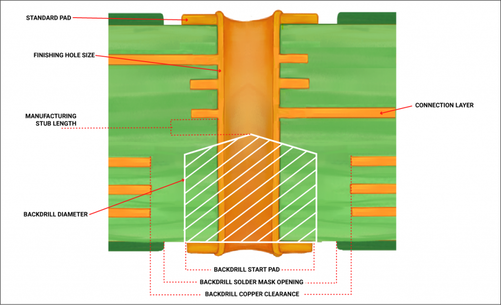
DFM guidelines for back drilling
The back drill diameter needs to be slightly larger than the primary drill diameter. The back drill bit size (diameter) is usually 8 mil over the primary drill size, with 10 mil larger preferred.
The table below provides a quick reference for backdrill clearances and drilling tolerances.
| Parameter | Recommended values |
|---|---|
| Backdrill-to-copper clearance | 10 mil |
| Backdrill-to-backdrill clearance | 6 mil |
| Min. backdrill oversize diameter | 8 – 10 mil |
| Min. depth for controlled depth drilling | >1 mil |
| Controlled depth drilling tolerance | ±2 mil |
Trace and plane clearances need to be large enough that the back-drilling process does not accidentally drill through traces and planes located adjacent to the back-drilled hole. Minimum plane and trace clearances (spacings) of 10 mil are preferred.
For more DFM tips, see Design for Manufacturing Handbook.

Design for Manufacturing Handbook
11 Chapters - 96 Pages - 90 Minute ReadWhat's Inside:
- Annular rings: avoid drill breakouts
- Vias: optimize your design
- Trace width and space: follow the best practices
- Solder mask and silkscreen: get the must-knows
Download Now
Advantages of back drilling PTH vias
- Via stubs give rise to a signal distortion issue named deterministic jitter. Jitter with regard to signal transmission in a PCB refers to timing errors caused by EMI, signal crosstalk, and noise. Deterministic jitter can be defined within the minimum and maximum variations.
- The Bit Error Rate (BER) is the number of bit errors per unit time and is largely dependent on deterministic jitter. Decreasing the deterministic jitter by back drilling will considerably decrease the overall BER of the signal.
- Reduces signal attenuation because of enhanced impedance matching and mitigates EMI/EMC radiation from the stub
- Reduces excitation of resonance modes.
- Decreases via-to-via crosstalk.
What is the maximum acceptable residual stub length after controlled depth drilling?
Residual stub lengths can range from 1 to 200 mil, with approximate signal loss increasing from 0.25% to 50%; however, most high-speed PCB designs target residual stub lengths of 10 mil or less to minimize signal integrity issues.
Once you decide to back drill, you will need to decide how much residual stub length can remain. The decision will depend on several interrelated factors, including the desired signal integrity performance and practical (cost-effective) manufacturing considerations and limitations.
Usually, increasing the number of vias that need to be back-drilled and decreasing the maximum residual stub length will increase the manufacturing costs of the PCB/backplane. Given below is a table that details the signal loss corresponding to a residual stub length.
| Remaining residual stub length (mil) | Approximate signal loss (%) |
|---|---|
| 1 | 0.25% |
| 2 | 0.5% |
| 5 | 1.25% |
| 10 | 2.5% |
| 20 | 5% |
| 40 | 10% |
| 60 | 15% |
| 100 | 25% |
| 200 | 50% |
Sierra Circuits fabricates and assembles high-quality circuit boards in the United States. Visit our PCB manufacturing capabilities to learn more.
How is controlled depth drilling implemented in Altium Designer?
Back drilling can be configured by defining the required layer pairs, assigning the target nets, setting maximum stub length and oversize parameters, and validating the resulting vias after routing. The following steps walk through the complete process in Altium Designer.
Step 1: Selecting the circuit segment
In this demonstration, we are choosing the Ethernet section, and within the Ethernet section, we are choosing the RX segment.

Before we take up routing, we need to carry out the back drill setup.
Step 2: Adding a back drill via
Go to Design and then Layer Stack Manager. Over here, we need to add a back drill via.

To do that, click the Features tab at the top right corner of the screen. Within the drop-down list, select the feature called Back Drills.

After that, at the bottom left portion of the screen, select the Back Drill tab. Once you click that, the back drill option is displayed. This is where you will get to add the various back drill parameters.

By clicking on the plus tab, you can add more back drills. You can also use the delete option shown with a bin symbol, to delete back drills you don’t require.
Step 3: Selecting the start and stop layer
In the Layer Stack Manager, you can select the First and Last layers from the Properties panel on the left side. Here we are selecting the top layer as the first layer and the fifth layer as the last layer. You can see that the backdrill figure will also change to reflect your selection of the first and last layers.

Now save your work in the Layer Stack Manager and click Close.

Next, go to Design and click on Net classes.

This will open the Object Class Explorer window. Then, right-click on Net classes and select add class in the drop-down menu. Now you need to name the class backdrill.

Now you need to add the nets that need backdrill vias. We will select the Ethernet RX nets and click on the > icon to add the nets as members for the backdrill operation. Click OK.

Step 4: Adding a design rule
Next, you need to set the stub length and the oversize parameters. Go to Design and then click Rules.

Back drilling addresses the issues regarding signal integrity and resonance in vias. Hence, manufacturers and designers need to consider the use of back drilling in order to maintain signal integrity in high-speed signal PCBs.
The PCB Rules and Constraints Editor will be displayed. Select High speed and click Maximum stub length.

Click the New Rule tab at the bottom of the screen.

The back drilling rule is then added. Now, double-click the rule to set the required values.
After this, select the net class and then select back drill. Click Apply, then OK. The next step is to perform the required routing.
We are going to keep the stub length as 15 mil. This is the oversize of the back drill, which we will set as 10 mil. The tolerance will be set as plus and minus 3 mil.

Step 5: Checking the back drills
Once the routing is done, we need to check if the back drills have been set properly. To check the same, switch on all layers. You can see that the circumference of the vias is displayed with dual colors.
In this case, the red color indicates the First Layer or start layer, and the blue color indicates the Last layer or stop layer.
You can clearly see the difference between the back-drilled vias and the other vias. Only the back-drilled vias show up in dual colors.

To view how many vias, PTH, and other holes have been drilled, select the Place option from the main menu and click Drill Table.

Step 6: Viewing the drill table
You can select and view vias according to their properties using the Property option and selecting the required Layer Pair. Here you can see the drill count is 12, the hole size is 30 mil, the type of plated hole is NPTH, and the drill hole tolerance as well.


Back drilling addresses the issues regarding signal integrity and resonance in vias. Hence, manufacturers and designers need to consider the use of back drilling in order to maintain signal integrity in high-speed signal PCBs.
Need help implementing back drilling for high-speed PCB designs? Our engineering team can assist you with controlled impedance optimization via stub reduction and manufacturing feasibility to improve performance.
You can book a meeting with our experts or call us at +1 (800) 763-7503.

Back drilling FAQs
Q1. Why is back drilling also called control depth drilling?
A: Back drilling is also known as controlled depth drilling, as these holes are back-drilled to a predetermined, controlled depth.
Q2. What is the maximum stub length that can be retained after back drilling without significantly affecting signal integrity?
A: 10 mil
Q3. Name alternate construction techniques that could be used to minimize stub length other than back drilling.
A: Laser-drilled vias (microvias), or blind and buried vias, and alternative stack-up arrangements where traces are moved to layers closer to the end of the via stub.
Q4. What is the main manufacturing parameter to consider in back drilling?
A: Hole depth or Z-axis depth.
Q5. Why are smaller stub lengths (<10 mil) hard to achieve during back drilling?
A: Minimizing stub length below 10 mil calls for more accuracy in the drill machine, which makes it more challenging. Also, it increases manufacturing costs; hence, it is difficult to reduce stub length. If your manufacturer is using the latest drilling equipment, there is a possibility of achieving 2 to 3-mil stubs. Check with your manufacturer.
Need assistance in designing your circuit board? Post your questions in the SierraConnect forum. Our experts will answer them.


Start the discussion at sierraconnect.protoexpress.com