


Contents

On-demand webinar
How Good is My Shield? An Introduction to Transfer Impedance and Shielding Effectiveness
by Karen Burnham
Signal integrity issues occur when a signal is distorted as it travels between the driver and receiver. Inconsistent impedance, closely spaced traces, and PDN noise can all degrade the quality.
These effects become more noticeable as rise times decrease. Shorter rise times have higher-frequency content, causing traces to behave like transmission lines.
As frequency increases, material selection, stack-up, and layout influence signal quality. A design that works reliably at lower speeds can develop reflections, timing errors, crosstalk, loss, or noise as edge rates increase.
For PCB designers and layout engineers, understanding these factors early in the design process helps maintain signal quality and avoid expensive design changes during fabrication and testing.
In this article, you’ll learn what causes signal integrity problems and how to prevent them.
Highlights:
- Match impedance to minimize signal reflections and discontinuities.
- Maintain 3W spacing and limit parallel routing to reduce crosstalk.
- Use continuous reference planes and short return paths to reduce noise, ground bounce, and EMI.
- Minimize via and trace stubs through proper routing, via structures, or backdrilling to reduce reflections and attenuation.
What is signal integrity in a PCB?
It is the ability of a signal to propagate from its driver to its receiver with its intended voltage, timing, and waveform characteristics without distortion. Signal integrity measures the amount of signal degradation when the signal travels from the driver to the receiver.
At lower speeds and with slower rise times, these effects may have little impact on circuit operation. As edge rates become faster, however, even relatively low-frequency digital signals can experience transmission-line effects that affect signal quality.

When a signal propagates from the driver to the receiver, it doesn’t remain the same; whatever has been sent originally will be received with varying degrees of distortion. This signal distortion happens due to factors like impedance mismatch, reflections, transient oscillations, crosstalk, ground bounce, and jitter in PCBs.
A designer’s primary aim should be to minimize such factors so that the original signal can make it to the destination with minimum distortion. Special care is also needed to maintain signal quality and to control its undesirable effects on electronic circuitry. Read our post on controlled impedance routing using Altium.
Why is signal integrity important in high-speed boards?
It is essential for reliable high-speed signal transmission because excessive waveform distortion, noise, and timing errors can cause unpredictable or intermittent behavior. Signal integrity problems may pass initial laboratory testing but appear during volume production, under different operating conditions, or when component lots change.
A signal loses integrity due to:
- Waveform distortion: The signal shape changes through ringing, overshoot, undershoot, or excessive rise/fall-time distortion, potentially violating logic thresholds or setup-and-hold timing requirements.
- SNR degradation: Unwanted electrical noise is superimposed on the signal, reducing its signal-to-noise ratio.
- Unwanted coupling: A signal generates crosstalk, ground bounce, or power disturbances that interfere with neighboring circuits.
A PCB has good signal integrity when it features:
- Clean propagation: High-speed signals reach their receivers without distortion or timing errors that affect circuit operation.
- Noise immunity: Traces and devices remain sufficiently immune to internal electrical noise and external electromagnetic interference.
- Electromagnetic compatibility (EMC): The layout controls emissions and return-current paths to meet applicable EMC requirements and regulatory limits.
Also read: 9 HDI Considerations for Manufacturability and Cost
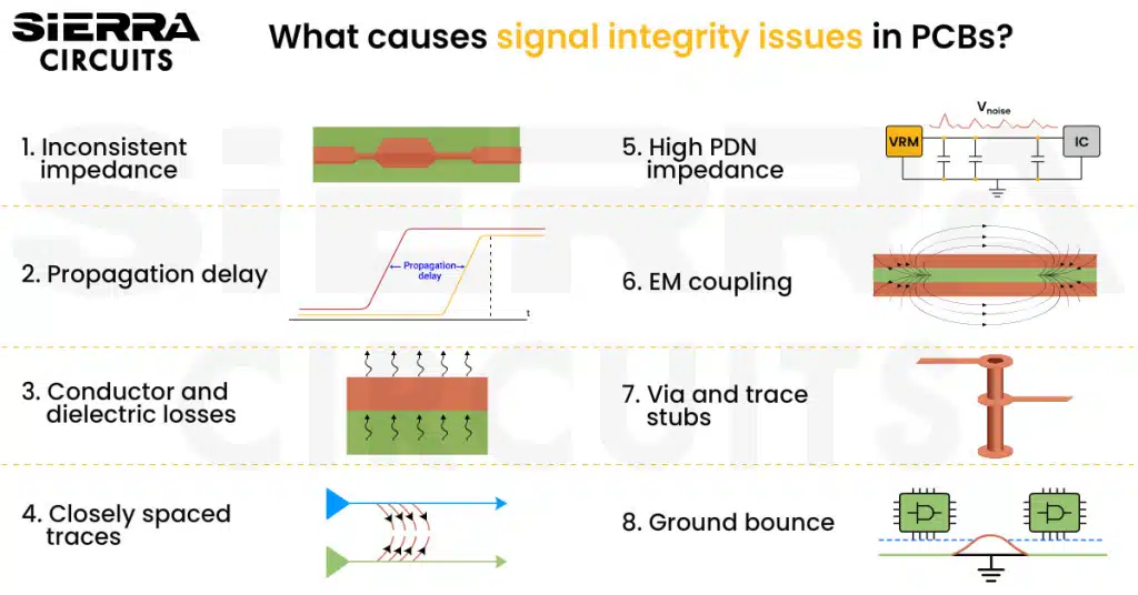
8 factors that lead to signal integrity issues in PCBs
The major factors that can affect signal integrity are uncontrolled impedance, impedance discontinuities, propagation delay, attenuation, crosstalk, power distribution, EMI/EMC, via and trace stubs, and ground bounce.
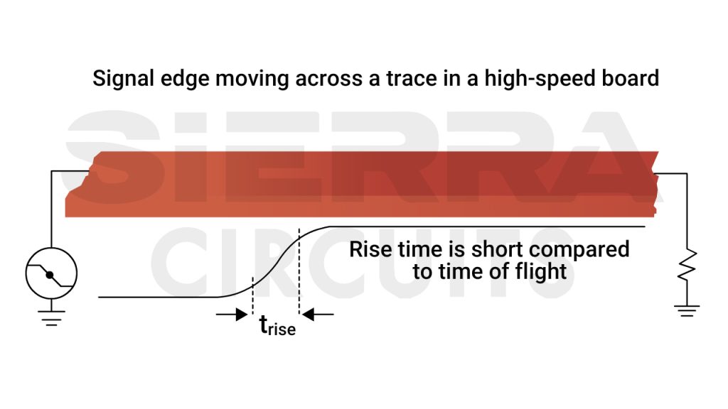
Perhaps the most important cause of transmission issues in a PCB is faster signal rise times. When circuits and devices are operating at low-to-moderate frequencies with moderate rise and fall times, problems due to PCB design are rarely an issue. However, when we are operating at high (RF and higher) frequencies, with much shorter signal rise times, signal integrity due to PCB design becomes a very big issue. As edge rates increase, PCB traces behave more like transmission lines, making their impedance, physical dimensions, return paths, and surrounding structures increasingly important.
To learn how to mitigate signal integrity challenges in high-density boards, read 10 HDI PCB design tips to maintain signal integrity.
Fast signal rise times and high signal frequencies increase issues.
For analytical purposes, we can divide various issues into the following categories:
1. Uncontrolled impedance causes signal reflections and ringing
Signal quality depends on the impedance characteristics of the trace and its return path. When impedance changes along the signal path, part of the signal reflects toward the source, causing ringing and signal distortion. The effect becomes more significant as the signal rise time decreases.
To minimize reflections caused by uncontrolled impedance:
- Maintain a uniform, controlled impedance along the signal path.
- Keep the return path continuous and close to the signal layer.
- Match the source and receiver impedances to the transmission-line characteristic impedance where required.
- Use an appropriate termination technique to reduce reflections.

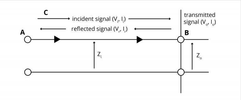
Any physical feature that changes the signal’s impedance can create reflections, ringing, and signal distortion. Discontinuities in the line’s impedance will occur at the point of encountering one of the following situations.
When a signal:
- Encounters a via in its path.
- Branches out into two or more lines.
- Stubs are connected to signal lines.
- Starts at the source end.
- Terminates at the receiver end.
- Return paths are connected to connector pins.
The faster the signal rise time, the greater the signal distortion caused by impedance discontinuities. We can minimize signal distortion due to line impedance discontinuities by:
- Minimizing the effects of discontinuities caused by vias and via stubs by using smaller microvias and HDI PCB technology.
- Reducing trace stub lengths.
- Routing traces in daisy chain fashion rather than multi-drop branches when a signal is used at more than one place.
- Implementing terminating resistors at the source and receiver ends.
- Using differential signaling and tightly coupled differential pairs, which are inherently more immune to discontinuities in signal return path planes.
- Ensuring that at connectors where discontinuity occurs, signal lines are made as short and signal return paths as wide as possible.
2. Propagation-delay mismatch causes timing errors
Signals take finite time as they travel on a PCB from source to receiver. The signal delays are directly proportional to signal line lengths and inversely proportional to signal speed on the specific PCB layers. If data signals and clock signals do not match overall delays, they would arrive at different times for detection at the receiver, and this would cause signal skew; excessive skew would cause signal sampling errors. As signal speeds become higher, the sampling rates are also higher, and allowable skew gets smaller, causing a greater propensity for errors due to skew.
To minimize propagation-delay mismatch:
- Match the delays of related signal and clock lines.
- Use trace-length matching where required.
- Account for differences between PCB layers when matching delays.
- Follow the interface-specific skew limits defined by the device or protocol.
3. Conductor and dielectric losses cause signal attenuation
Signals suffer attenuation as they propagate over PCB lines due to losses caused by conducting trace resistances (which increase at higher frequencies due to the skin effect) and the dielectric material dissipation factor Df. Both these losses increase as frequency increases; therefore, higher-frequency components of signals will suffer greater attenuation than do the lower-frequency components; this causes a reduction in signal bandwidth, which then leads to signal distortion by the increase in signal rise time, and excessive signal rise time increase results in errors in data detection.
To minimize signal attenuation:
- Select a low-loss PCB material.
- Control trace geometry to reduce conductor losses.
- Use shorter signal paths where practical.
- Consider frequency-dependent conductor and dielectric losses during material selection.
4. Closely spaced traces cause crosstalk
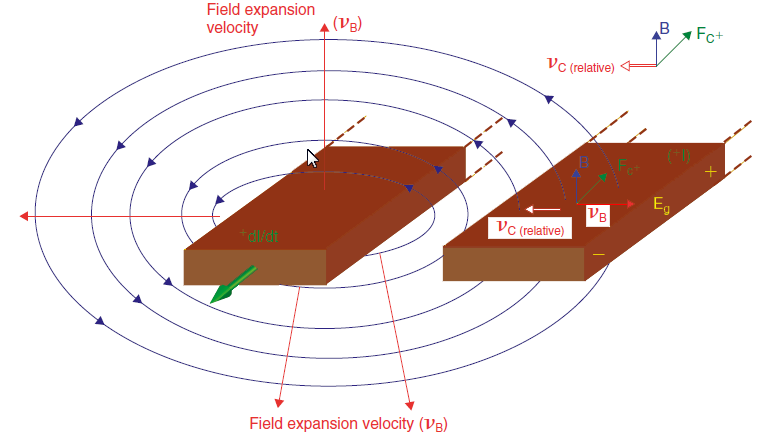
A fast voltage or current transition on a signal line or return path plane may couple onto adjacent signal lines, causing unwanted signals called crosstalk and switching noise on the adjacent signal lines.
The coupling occurs due to mutual capacitance and mutual inductance between the traces.
This mutual capacitive and inductive coupling can be reduced by increasing the space between the traces. As a thumb rule, space should be three times the trace width (3W).
Crosstalk and switching noise can be reduced by:
- Increasing the separation between adjacent signal traces.
- Making the signal return paths as wide as possible and uniform, like uniform planes, and avoiding split return paths.
- Employing a lower dielectric constant PCB material.
- Using differential signaling and tightly coupled differential pairs, which are inherently more immune to crosstalk.
5. PDN impedance causes power and ground noise
Power and ground rails, paths, or planes have very low but FINITE nonzero impedances. When output signals and internal gates switch states, currents through power and ground rails/paths/planes change, causing a voltage drop in power and ground paths. This will decrease the voltage across the power and ground pins of the devices.
The higher the frequency of such instances, the faster the signal transition times, and the higher the number of lines switching states simultaneously, the greater the voltage decrease across power and ground rails. This will reduce signals’ noise margins and, if excessive, will cause devices to malfunction.
To reduce these effects, the power distribution network has to be so designed as to minimize the power system’s impedance:
- Keep power and ground planes close together to reduce loop inductance.
- Place low-inductance decoupling capacitors close to device power and ground pins.
- Employ packages with short power and ground connections.
- Use thin, high-capacitance dielectric layers between power and ground planes where appropriate. Read how we can reduce parasitic capacitance in PCB layout.
6. EM coupling introduces unwanted noise
EMI and EMC problems become more significant as signal frequency and rise time increase. Fast-changing currents can radiate electromagnetic energy or couple unwanted noise into nearby circuits. Reducing the current-loop area helps limit this radiation.
Radiation far-field strength increases linearly with frequency for single-ended signal currents and quadratically with differential signal currents. Read PCB design guidelines for EMI and EMC for a detailed explanation.
To reduce EMI:
- Minimize high-frequency current-loop areas.
- Have continuous return paths.
- Keep high-speed signal and return paths closely coupled.
- Avoid unnecessary discontinuities in the signal and reference planes.
High-Speed PCB Design Guide
8 Chapters - 115 Pages - 150 Minute ReadWhat's Inside:
- Explanations of signal integrity issues
- Understanding transmission lines and controlled impedance
- Selection process of high-speed PCB materials
- High-speed layout guidelines
Download Now
7. Via and trace stubs cause reflections
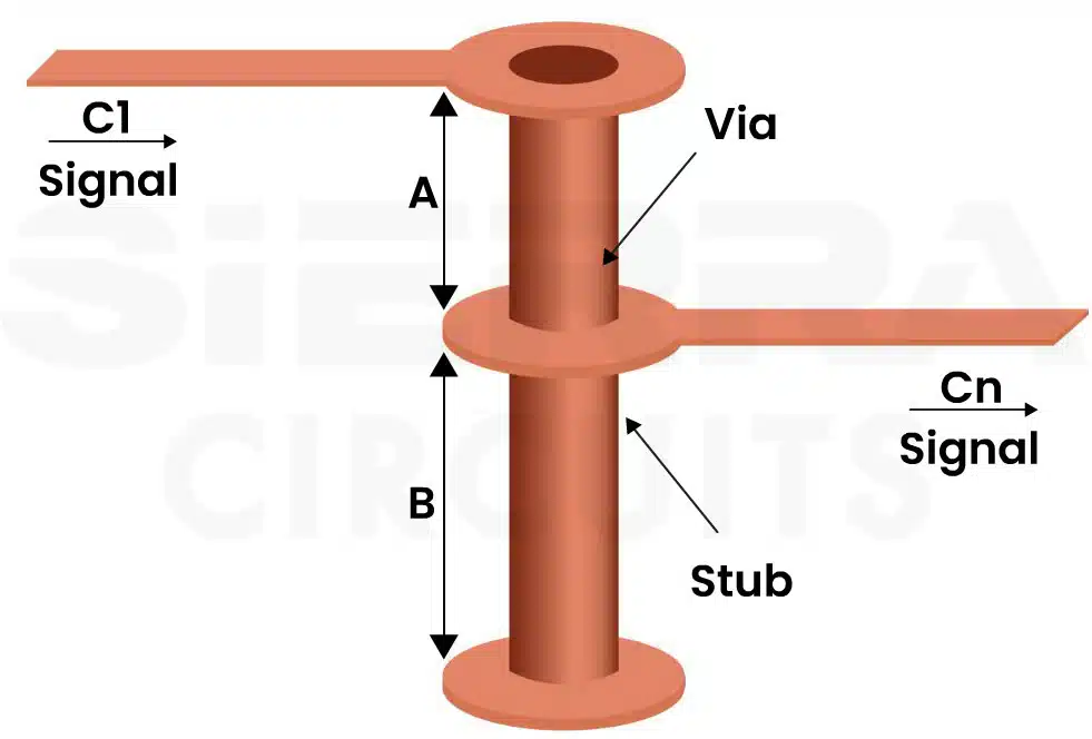
A via stub is the part of a via that is not used for signal transmission. A via stub acts as a resonant circuit with a specific resonant frequency at which it stores maximum energy within it. If the signal has a significant component at or near that frequency, that component of the signal will be heavily attenuated due to the energy demands of the via stub at its resonant frequency.
In the example depicted below, part A of the via is used for signal propagation from the conductor C1 on an outer layer to the conductor Cn on an inner layer. But part B of the via is extraneous; thus, it is the via stub. Learn more about Via Stubs and Their Effects on Signal Attenuation and Data Transfer Rates here.
Long stub traces may act as antennas and consequently increase problems in complying with EMC standards.
Stub traces can also create reflections that negatively affect signal integrity. Pull-up or pull-down resistors on high-speed signals are common sources of stubs. If such resistors are required, then route the signals as a daisy chain.
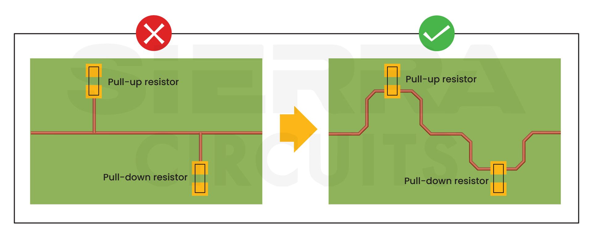
To minimize stub-related problems:
- Minimize trace stubs and nd keep via stubs as short as possible.
- Employ back-drilling or other suitable techniques to remove unused via sections.
- Use daisy-chain routing instead of unnecessary branches.
- Keep pull-up and pull-down resistor connections short on high-speed signals.
8. Ground bounce shifts the reference voltage
Ground bounce occurs when rapid current transitions create transient voltage spikes across the parasitic inductance and resistance of the ground path. This shifts the local ground reference level across different points on the PCB, reducing noise margins and causing false logic switching or timing errors.
To reduce ground bounce:
- Place decoupling capacitors as close as possible to IC power and ground pins to minimize loop inductance.
- Insert series damping resistors on switching lines to limit peak current and slow excessively fast edge rates.
- Use solid, unbroken ground reference planes rather than narrow ground traces.
- Place multiple ground vias close to IC pads to lower total return path inductance through parallel paths.
Signal integrity problems become more difficult to control as signal rise times decrease. Maintaining controlled impedance, continuous return paths, appropriate propagation delay, low-loss materials, adequate trace spacing, and a low-impedance PDN can prevent many of these issues during PCB design.
Addressing these issues during the design phase is more effective than correcting problems after fabrication. Plan the stack-up, routing, return paths, and power distribution early to reduce redesigns and improve overall system reliability.
About Rahul Shashikanth : Rahul Shashikanth is an electronics and communication engineer with over 8 years of experience in publishing technical articles on PCB design, manufacturing, and assembly. He is currently the content marketing manager at Sierra Circuits.






Start the discussion at sierraconnect.protoexpress.com