


Contents

On-demand webinar
How Good is My Shield? An Introduction to Transfer Impedance and Shielding Effectiveness
by Karen Burnham
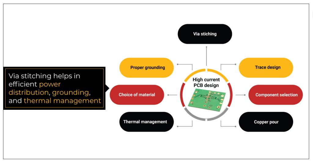
Via stitching in high-current PCBs helps in creating proper ground connections, power distribution, and heat dissipation. These boards carry high currents (more than 500 amps) and hence you need to be more cautious while designing them. In this article, you will learn via stitching and other strategies to build an efficient high-current circuit board.
What are high-current PCBs?
As the name suggests, these boards are built for high-current applications that handle more than 500 A and up to 1000 A. They have thicker copper features (traces, buses, bars, and copper pours), heavier copper layers (power and ground planes), and strong connection points. Additionally, these circuit boards are also capable of withstanding higher temperatures for a longer duration.
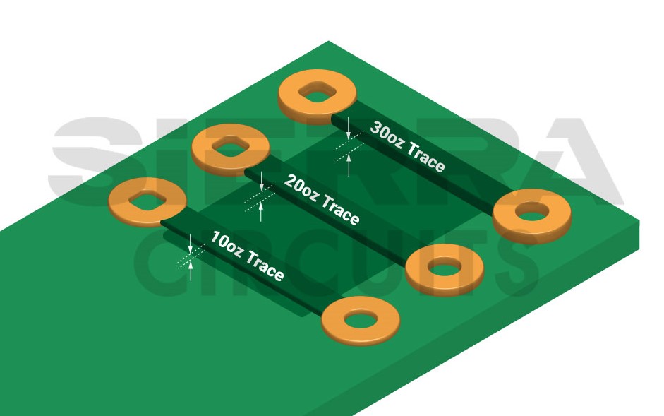
If more than 3 oz of copper is incorporated, it is referred to as a heavy copper PCB. High-current circuits can have 10 oz per square foot or more. Manufacturers use special etching/plating processes for the traces, holes, and via side walls to add extra copper thickness.
For expert insights into wet and dry PCB etching technologies, read the future of PCB etching by Laurent Nicolet.
Advantages of high-current boards
Standard boards will have difficulty managing increased currents which can lead to burnout. On the contrary, high-current boards can easily handle hundreds of amps and increased temperatures. Other advantages include:
- The circuit is designed to have greater trace and via current capacity.
- You can accommodate different current levels on the same layer.
- As larger copper features are fitted into smaller spaces, it improves the mechanical strength of the connectors.
- With proper design techniques, copper features (high-heat conduction materials) can divert excess heat from sensitive components. This reduces the risk of component failures or burnouts.
Challenges in designing high-current PCB layouts
While designing a high-current board, you will come across a unique set of hurdles, unlike standard boards.
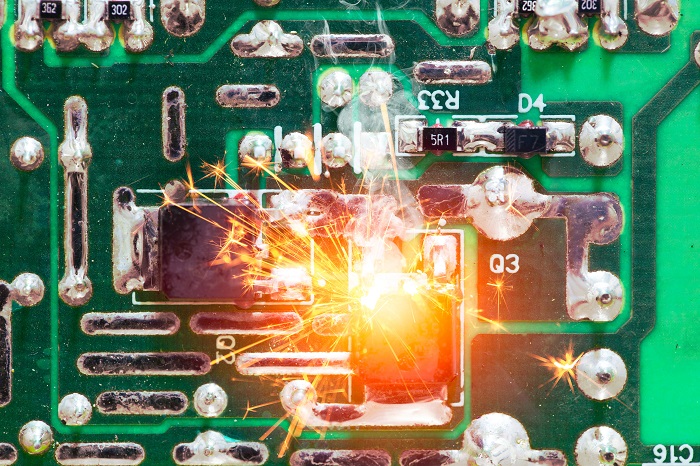
- The board can produce excess heat and electrostatic energy, which can cause design failures.
- If enough metal is not used in the power planes, it will cause the traces to burn out.
- Maintaining low inductance at the power supply is challenging. If a low inductance path is not maintained, you need to implement more decoupling capacitors to restore balance.
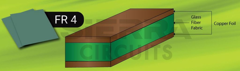
- Efficient thermal management is essential to avoid structural failures of the board. For instance, FR-4 has a glass transition temperature (Tg) of 130°C. If the board heat reaches beyond this temperature, it will lose its stability and starts to melt. Even before reaching this temperature, the traces on the board can melt and cause an open circuit.
- Higher current increases EMI in the circuit, especially in switching devices.
- These circuits can have safety and reliability issues. Any exposed features can cause electric shocks that can be detrimental to operators.

Design for Manufacturing Handbook
11 Chapters - 96 Pages - 90 Minute ReadWhat's Inside:
- Annular rings: avoid drill breakouts
- Vias: optimize your design
- Trace width and space: follow the best practices
- Solder mask and silkscreen: get the must-knows
Download Now
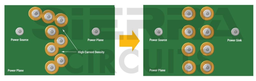
Implementing via stitching in high-current PCBs
Managing power and ground is essential while creating a high-current circuit design. Via stitching is one of the best ways to distribute heat formed due to the current flow.
What is via stitching?
It is a technique implemented to connect larger copper areas on different layers. Here, you add an array of vias and connect them to the ground or power planes. Adding these along the board’s surface creates a robust vertical connection through the structure. This will help to maintain a low impedance and short return loops.
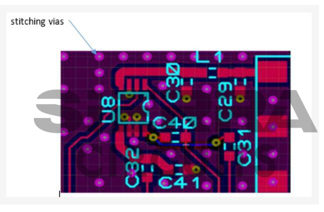
Designing via stitches for high-current PCB layout
Via stitching is implemented for various reasons. A few of them are summarized below.
Power distribution through multiple layers
Many systems demand high power for operation, and circuit boards embedded in them have to conduct high currents. These large currents can create noise. This can be controlled to a certain extent by using filters.
Another method is to place the component of a power supply circuit as close as possible while maintaining the DFM rules. You have to keep the trace short and wide to have a low-impedance path and reduce EMI. However, routing these high-current lines to other points on the board still remains a challenge. For this, using as much copper as possible will reduce heat and inductance. Adding metal to a single layer may not be sufficient. You need to route it through multiple layers.
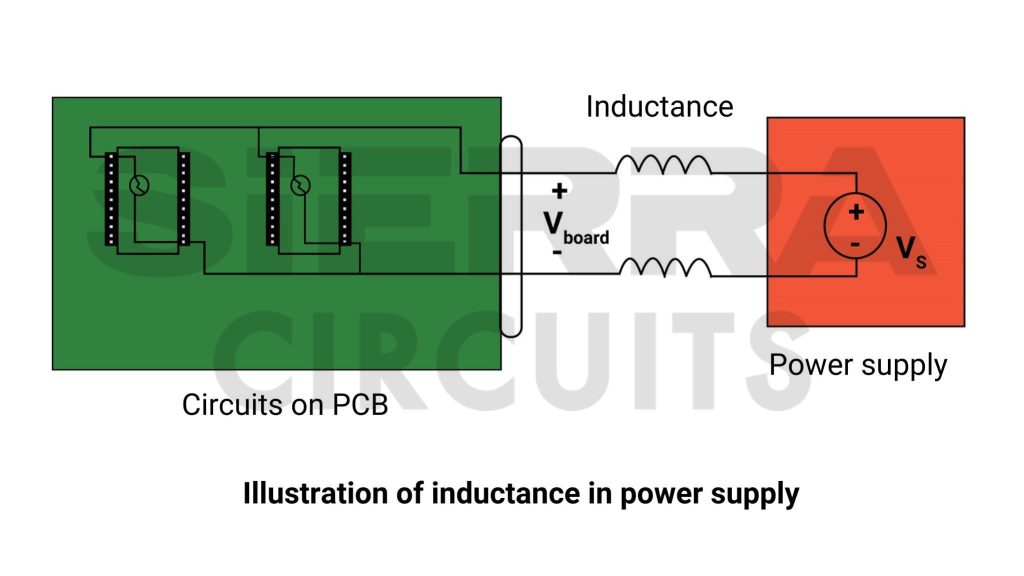
You can overcome these challenges by implementing via stitching. Connecting the power conductors through different layers using via will increase the trace current capacity. The array of vias can help in creating a low-resistance transition path for power nets. This will allow high-current to propagate with less loss across the layers. This also provides more space for routing or mounting components.

Efficient thermal management
High current traces induce a lot of heat. On the inner layers, if you stitch power traces with vias, it will add more metal to dissipate the heat. You can implement thermal via stitches connecting to an external layer. Thermal stitching vias are crucial for creating heat sinks. It is implemented to provide excellent thermal conductivity over different copper planes.
Grounding traces and copper pours
This is one of the widely used applications for via stitching. It provides a short ground return path for the circuit traces. It connects the ground across multiple layers. Hence, providing multiple parallel paths of low resistance and impedance across the different layers.
You can tie the copper pour to the ground using arrays of via. For designing a copper pour feature perfectly, it is essential to have via stitches with sufficient clearance. This not only connects the pour to the ground, but it also helps in providing better heat dissipation.
Shielding from EMI
Via stitching does provide protection from EMI, but only up to a certain frequency. Usually, single or multiple rows of vias are stitched across the required parameter. The vias avoid the coupling of EM waves into victim traces. Vias create a shield as its loop inductance is lower since it is connected to the ground.
See our case study on designing a high-current PCB with voltage doublers to learn how we estimated the number of vias for stitching at multiple current levels.
PCB layout design guidelines for via stitching
- Leave enough space around the components for placing the vias especially if you are grounding or dissipating the heat of a large component on the board.
- If sufficient clearance is not provided between vias, it can lead to crosstalk. In low-frequency designs, it is advised to maintain a spacing of λ/20, while for high-frequency circuits, a spacing of λ/10 between stitching vias is recommended. Here, λ represents the operational wavelength of the signal.
- Apart from board thickness, board size also affects the number of vias you can accommodate in the layout.
- If your PCB has to operate in a harsh environment with high power and temperatures, you need to alter your design accordingly. You may have to implement more grounding and thermal stitching vias for safety and stability.
- All the EDA tools like Altium Designer, Allegro, and KiCad have built-in tools for implementing via stitches in the design. While designing them, the via size, spacing, and grid arrangement become crucial. Read PCB via design using Altium Designer for more.
As discussed above, via stitching is used for different applications like thermal management, EMI shielding, and power/ground net distribution. The design methods for all these applications will be different. While connecting these vias, ensure that you are not overlapping with other interconnections or connecting to a different layer. EDA software packages provide automatic via stitching options, which can be helpful while designing.
KiCad Design Guide
10 Chapters - 161 Pages - 180 Minute ReadWhat's Inside:
- Creating a component symbol library
- Setting up board parameters and rules
- How to route differential pairs
- How to place of components
Download Now
More design tips for high-current PCBs
When designing a high-current circuit board, keeping the design as simple as possible will be practical and cost-effective. Here are a few essential design tips:
Pick special dielectrics materials for higher temperatures
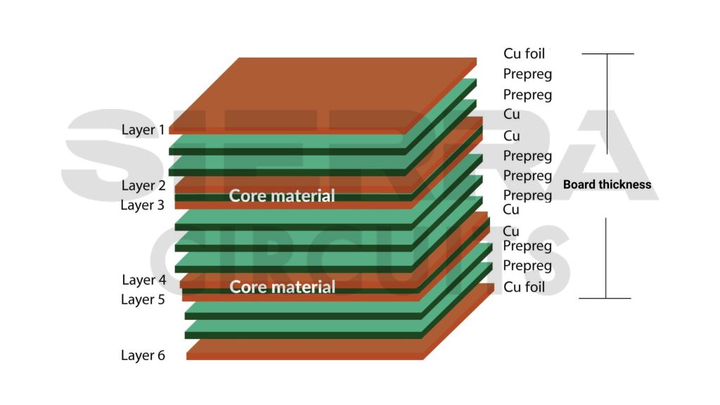
The chosen PCB material must endure the increased heat produced by high currents. It is good to explore special dielectrics that can endure higher temperatures during operation. Even if these materials are expensive, they can help you avoid thermal-related issues. You should also pay attention to the thermal expansion between copper and the dielectric to prevent damage or cracks on the substrate. It is recommended to work closely with your manufacturer when building the stack-up for your high-current boards.
Shorter traces for high-current design
Trace length and width: The power loss at the trace becomes extremely crucial for high-current PCB connectors. Longer traces have more resistance with increased power loss and heat dissipation. Hence, shorter traces will be a better choice. Additionally, power loss can be reduced by employing a wider conductor cross-sectional area. So, heavier copper and wider traces are essential. Ensure that the copper density is not less than 35–50 microns (3–4 oz/ft2).

Alternates for high-current traces: Opt for solderable copper bars or buses that can withstand larger currents. In cases of high currents in power systems, replace the traces with a power plane if possible.
Remove solder mask: One way of improving the trace current capacity is by stripping the solder mask. This will ensure the connectivity of the trace. It will also reduce the resistance of the conductor.
Go for a thicker circuit board
Even though thinner boards provide better heat conductivity, with a thicker board, you can have heavier copper. This increases the thickness of your trace and allows you to have a lower conductor width with the same current-carrying capacity. This will provide more space on the board for component placement. Hence, thicker boards are a better choice for high-current circuits.
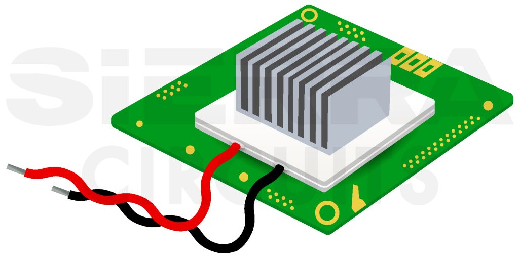
Thermal management strategies
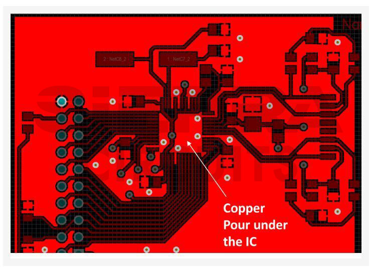
The heat produced in high-current circuit boards is very high, so you cannot depend on natural convection for thermal dissipation. Components like amplifiers, regulators, and converters are very sensitive to stress and pressure in their surroundings. This can cause faults in the circuit. Hence, it is good to separate these parts and provide thermal isolation.
You can provide thermal isolation by avoiding a polygon pour under the component and instead opting for thermal relief connections. An alternative method is to create a cutout to separate sensitive components from other parts that dissipate heat. You can also implement large heat sinks or provide a direct conduction path to improve the heat dissipation in the overall circuit. Read 12 PCB thermal management techniques to learn more.
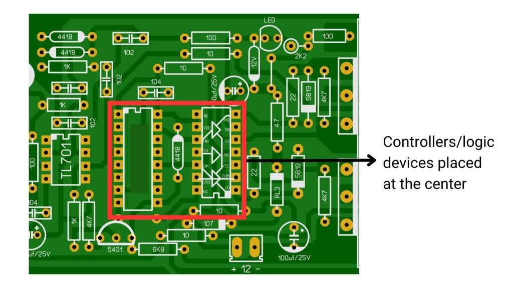
Place high-current components at the center
While selecting components, checking the ratings is crucial. Always be aware of the current ratings and thermal resistance of MOSFETS, connectors, terminals, and inductive components. Knowing the operating current and thermal resistance will help in creating robust thermal management. Parts carrying high currents (microcontrollers and microprocessors) should be placed in the center of the board and not at the edges for better heat dissipation.
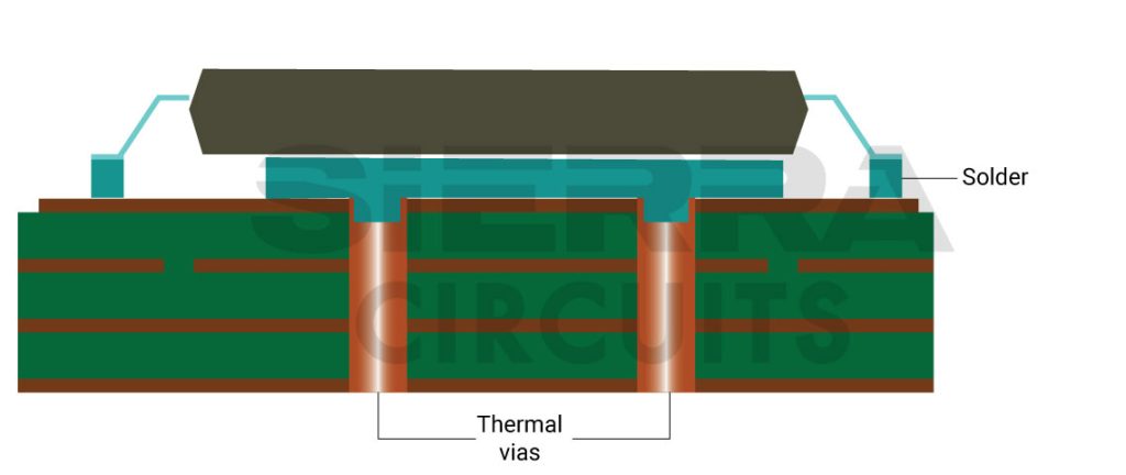
Implement thermal relief pads for heat management
As mentioned, high-current boards have wider and thicker copper features for improving current capacity and heat dissipation. However, these large metal areas can create a thermal imbalance during the soldering process. To establish reliable solder joints, implement thermal relief pads while connecting components directly to metal features or wider traces.
When designing a high-current PCB, you can come across many challenges in routing, component placement, and thermal management. However, by implementing the right design techniques, like via stitching, thicker trace routing, proper grounding techniques, etc., you can build a reliable board. If you require any guidelines for designing high-current boards, let us know in the comments. Our design team will be happy to help you out.
Need help in designing reliable PCBs? Our engineering team can help you with thermal management, stack-up design, and DFM analysis.
You can book a meeting with our experts or call us at +1 (800) 763-7503.

About Sushmitha V : Sushmitha V has a master's degree in power electronics and has over four years of experience in the PCB industry. Her areas of interest include circuit board manufacturing, assembly, IPC standards, and DFM/DFA practices.


