


Contents

On-demand webinar
How Good is My Shield? An Introduction to Transfer Impedance and Shielding Effectiveness
by Karen Burnham
Controlled impedance (CI) in PCBs is important to minimize signal reflections, timing errors, and maintain signal integrity. As a designer, understanding the concept of uniform impedance helps you create reliable high-speed circuit boards.
Highlights:
- CI is the impedance of transmission lines, essential for high-speed signal propagation.
- Impedance variation is influenced by the materials’ resin content, dielectric constant (Dk), glass weave type, and physical trace tolerances.
- Maintain a minimum spacing of 3W between adjacent traces to reduce the risk of crosstalk.
- Length matching of differential pairs is essential to minimize delay skew.
In this article, you’ll learn why controlled impedance is critical in high-speed designs, along with practical tips for routing these traces.
What is controlled impedance?
It is the characteristic impedance of a transmission line formed by traces and their associated reference planes. It is relevant when high-frequency signals are propagating on circuit boards.
The impedance of circuits is determined by the physical dimensions and the dielectric materials. It is measured in Ohms (Ω).
The types of PCB transmission lines that require uniform impedance are:
- Single-ended microstrip
- Single-ended stripline
- Microstrip differential pair
- Stripline differential pair
- Embedded microstrip
- Co-planar (single-ended and differential)
Consistent impedance is important for solving signal integrity problems.
Why do you need controlled impedance?
Uniform impedance is required to ensure signals travel cleanly, without reflections, distortion, or timing errors.
Typically, you will need uniform impedance for circuit boards used in high-speed digital applications, such as RF communication, telecommunications, computing using signal frequencies above 100MHz, high-speed signal processing, and high-quality analog video, such as DDR, HDMI, Gigabit Ethernet, etc.
At high frequencies, the traces act like transmission lines, which have impedance at each point on the signal trace trajectory. If this impedance varies from one point to the next, there will be a signal reflection whose magnitude will depend on the difference between the two impedances.
The larger the difference is, the greater the reflection will be. This reflection will travel in the opposite direction of the signal, which means that the reflected signal will superimpose on the primary signal.
As a result, the original signal will be distorted: the signal intended to be sent from the transmitter side will have changed once it gets to the receiver side. The distortion may be so much that the signal may not be able to perform the desired function.
Therefore, traces must have uniform impedance to minimize signal distortions caused by reflections. This is the first step to improving the integrity of the signals on the traces. For a better understanding, read the effects of high-speed signals in a PCB design.
A uniform transmission line on a printed board has a definite trace width and height and is at a uniform distance from the return path conductor, usually a plane at a certain distance from the signal trace.
For more, download the Controlled Impedance Design Guide.

Controlled Impedance Design Guide
6 Chapters - 56 Pages - 60 Minute ReadWhat's Inside:
- Understanding why controlled impedance is necessary
- Stack-up design guidelines
- How to design for impedance
- Common mistakes to avoid
Download Now
4 factors that affect the impedance of a transmission line
The uniform impedance of a trace is influenced by:
-
- Materials’ resin content percentage
- Dk values of the resin
- The type of glass cloth used
- Physical tolerances like trace height and width at the top and bottom of the trace.
The tables below show a list of cores and prepregs commonly used by Sierra Circuits for controlled impedance designs.
| Material name | Construction | Resin content (%) | Dissipation factor (Df) @10 GHz | Dielectric constant (Dk) @10 GHz | Thickness (mil) |
|---|---|---|---|---|---|
| FR370HR | 1 x 10⁶/1 x 1080 | 60 | 0.026 | 3.84 | 4 |
| 2 x 1080 | 55 | 0.025 | 3.99 | 4.5 | |
| 1 x 2116 | 54 | 0.024 | 3.96 | 5 | |
| VT47 | 1 x 2116 | 45 | 0.016 | 4.15 | 4 |
| 1 x 2116 | 55 | 0.018 | 3.9 | 5 | |
| 1 x 2112 | 52 | 0.017 | 4 | 6 | |
| FR408HR | 1 x 10⁶+1 x 1080 | 59 | 0.0096 | 3.54 | 4 |
| 1 x 10⁶+1 x 1080 | 62 | 0.0098 | 3.48 | 4.5 | |
| 1 x 2116 | 54 | 0.0093 | 3.67 | 5 | |
| I-Speed | 2 x 1035 | 67 | 0.0059 | 3.55 | 4 |
| 2 x 1067 | 69.3 | 0.0059 | 3.51 | 4.5 | |
| 2 x 1067 | 72 | 0.0059 | 3.45 | 5 | |
| N7000-2HT | 1 x 10⁶+1 x 1080 | 56 | 0.0147 | 3.7 | 4 |
| 2 x 1080 | 51 | 0.014 | 3.86 | 4.5 | |
| 1 x 2113 + 1 x 10⁶ | 53 | 0.0143 | 3.79 | 5 | |
| Megtron 6 R-5775 (K) | 2 x 1035 | 65 | 0.004 | 3.37 | 3.9 |
| 1 x 2116 | 54 | 0.004 | 3.61 | 4.9 | |
| 2 x 1080 | 63 | 0.004 | 3.39 | 5.9 | |
| I-Tera MT40 | 2 x 1035 | 65.5 | 0.0025 | 3.26 | 4 |
| 2 x 1067 | 70.5 | 0.0023 | 3.18 | 5 | |
| 2 x 1086 | 61 | 0.0028 | 3.32 | 6 | |
| Tachyon 100G | 2 x 1067 | 66.5 | 0.0017 | 3.05 | 4 |
| 2 x 1067 | 70 | 0.0016 | 3.02 | 4.5 | |
| 2 x 1067 | 72.5 | 0.0015 | 2.98 | 5 | |
| Astra MT-77 | 1 x 5 mil core | – | 0.0017 | 3 | 5 |
| 1 x 7.5 mil core | – | 0.0017 | 3 | 7.5 | |
| 1 x 10 mil Core | – | 0.0017 | 3 | 10 | |
| Rogers 4350B | 1 x 4 mil core | – | 0.0017 | 3.33 | 4 |
| 1 x 6.6 mil core | – | 0.0017 | 3.48 | 6.6 | |
| 1 x 8 mil core | – | 0.0017 | 3.48 | 8 |
| Material name | Glass weave | Resin content (%) | Dissipation factor (Df) @10 GHz | Dielectric constant (Dk) @10 GHz | Thickness (mil) |
|---|---|---|---|---|---|
| FR370HR | 106 | 76 | 0.031 | 3.54 | 2.4 |
| 1080 | 71 | 0.03 | 3.63 | 3.6 | |
| 2113 | 59 | 0.026 | 3.86 | 4 | |
| VT47 | 106 | 76 | 0.021 | 3.35 | 2.5 |
| 1080 | 64 | 0.019 | 3.65 | 3 | |
| 2113 | 57 | 0.018 | 3.83 | 4 | |
| FR408HR | 106 | 75 | 0.011 | 3.22 | 2.3 |
| 1086 | 65 | 0.01 | 3.42 | 3.5 | |
| 1080 | 71 | 0.011 | 3.3 | 4 | |
| I-Speed | 1035 | 71.5 | 0.0059 | 3.46 | 2.4 |
| 1078 | 69.5 | 0.0059 | 3.5 | 3.6 | |
| 1086 | 70 | 0.0059 | 3.49 | 4 | |
| N7000-2HT | 106 | 72 | 0.0166 | 3.33 | 2.3 |
| 1080 | 68 | 0.0161 | 3.41 | 3.9 | |
| 2113 | 55 | 0.0146 | 3.83 | 4.2 | |
| Megtron 6 R-5670 (K) /R-5775(K) | 1035 | 70 | 0.004 | 3.19 | 2.36 |
| 1078 | 68 | 0.004 | 3.32 | 3.5 | |
| 1078 | 72 | 0.004 | 3.22 | 4.1 | |
| I-Tera MT40 | 1067 | 69 | 0.0024 | 3.24 | 2.4 |
| 1078 | 69 | 0.0024 | 3.22 | 3.7 | |
| 1080 | 73 | 0.0022 | 3.12 | 4.2 | |
| Tachyon 100G | 1067 | 71.5 | 0.0016 | 3.02 | 2.4 |
| 1078 | 70.5 | 0.0016 | 3.04 | 3.5 | |
| 1078 | 75 | 0.0014 | 2.97 | 4.2 | |
| Astra MT-77 | 1067 | 72 | 0.0019 | 2.98 | 2.5 |
| 1078 | 70 | 0.0019 | 3.01 | 3.6 | |
| 1078 | 74 | 0.0019 | 2.95 | 4.2 | |
| Rogers 4450T | 106 | 82 | 0.0039 | 3.23 | 3 |
| 1035 | 75 | 0.004 | 3.35 | 4 | |
| 1065 | 80 | 0.0038 | 3.28 | 5 |
When you provide Sierra Circuits with your PCB design, including copper patterns, hole layouts, and final material thicknesses, we laminate the copper layers into a single circuit board. We manufacture your circuit board with precise pattern dimensions and placements, maintained within specified tolerances.
You must ensure that your manufacturer provides you with the right size, position, and tolerance for your etched features. If not, your boards will vary from each other, making debugging performance-related issues very difficult.
Why controlled impedance is a better choice than controlled dielectric
Specifying the dielectric instead of CI gives you theoretical control, but it also puts the responsibility for accuracy and manufacturability entirely on you.
When you choose a controlled dielectric approach, you’re defining circuit board material properties (dielectric constant, glass style, resin content, and layer spacing) and calculating the impedance yourself. That means you must ensure every variable (trace width, spacing, and stack-up tolerances) stays within limits during fabrication. Any deviation can shift the final impedance, and the risk of mismatch increases.
On the other hand, specifying impedance shifts the responsibility to the manufacturer. We adjust the stack-up, materials, and trace geometry as needed to meet your target impedance within tolerance, ensuring consistent electrical performance.
Controlled dielectric offers more direct control for those comfortable with detailed calculations; controlled impedance is typically the safer and more reliable choice for achieving consistent results.
For advanced trace design tips, see 10 best layout tips for high-speed and high-current PCB traces.

How to design a board with uniform impedance?
You can create a board with uniform impedance by carefully defining the stack-up, trace geometry, and dielectric materials to achieve target impedance values.
Follow the below-mentioned controlled impedance routing strategies when designing the layout:
1. Determine which signals require uniform impedance
Most of the time, electrical engineers specify which signal nets require a specific impedance. However, if they do not, the designer should review the datasheets of the integrated circuits to determine which signals require uniform impedance.
The datasheets usually provide detailed guidelines for each group of signals and their impedance values. The spacing rules and information on which layer to route specific signals may also appear in the datasheets or in the application notes. DDR traces, HDMI traces, Gigabit Ethernet traces, and RF signals are some examples of controlled impedance traces.
2. Annotate the schematic with impedance requirements

The design of a board starts with the design of the circuit schematics by the design engineer. The engineer must specify impedance signals in the schematic and classify specific nets to be either differential pairs (100, 90, or 85 ohms) or single-ended nets (40, 50, 55, 60, or 75 ohms).
It’s a good design practice to add an N or P polarity indication after the net names of the differential pair signals in a schematic. The engineer should also specify particular impedance layout design guidelines (if any) to be followed by the layout designer, either in the schematic or in a separate “Read Me” file.
3. Identify the trace parameters for controlled impedance
A PCB trace is defined by the thickness, height, width, and dielectric constant (Er) of the material on which the traces are etched. While designing controlled impedance boards, it is essential to take care of these parameters.
You can provide the manufacturer with the number of layers, the value of the impedance traces on specific layers (50 or 100 Ω on layer 3), and materials.
The manufacturer gives you the stack-up that mentions the trace widths on each layer, the number of layers, the thickness of each dielectric in the stack-up, the trace thickness, and the material. They also take care of the controlled impedance requirements by calculating the feasible thickness, width, and height for the traces that need impedance control.
Understand how impedance varies with physical parameters by following these relationships:
- Impedance is inversely proportional to trace width and trace thickness.
- Impedance is proportional to the laminate height, and it is inversely proportional to the square root of the laminate’s dielectric constant (Er).
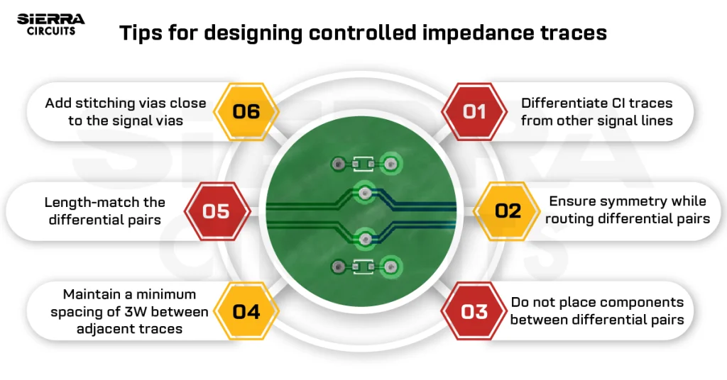
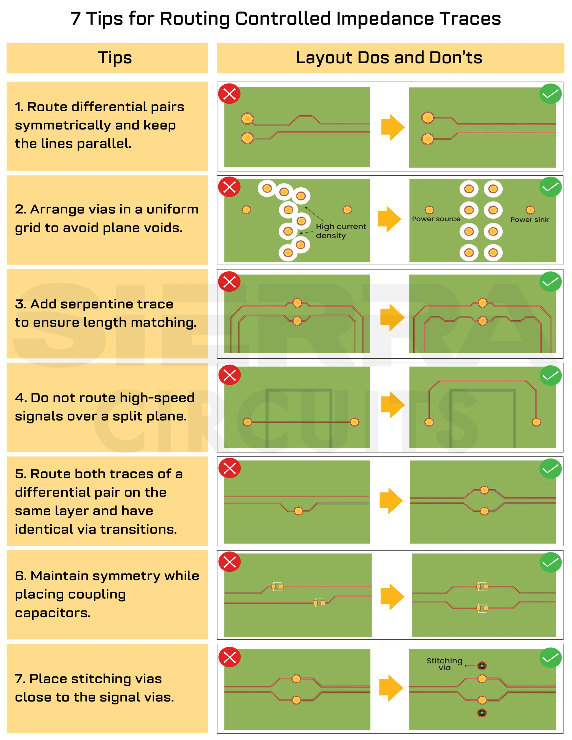
7 tips for designing controlled impedance traces in PCBs
The following infographic shows the dos and don’ts for routing controlled-impedance traces.
1. Differentiate controlled impedance traces from other signal lines
The controlled impedance trace widths must be distinguishable from the remaining traces on the board. It allows the manufacturer to quickly identify them and make suitable changes to the trace width, if necessary, to achieve a specific impedance.
For example, if you require a 5 mil trace to achieve 50 Ω impedance and if you have also routed other signals with 5 mil width, it will be impossible for the board manufacturer to determine which ones are the impedance traces. Therefore, you should make the 50 Ω impedance traces 5.1 mil or 4.9 mil wide.
The table below shows trace widths and spacings for uniform impedance on different layers. Non-impedance signal traces should not be routed with 3.5, 3.6, 4.2, 4.25, and 4.3mil trace widths.
| Layer | 50 Ω (SE) (mil) | Differential pair 90 Ω | Differential pair 100 Ω | ||
|---|---|---|---|---|---|
| 90 Ω trace (mil) | 90 Ω space (mil) | 100 Ω trace (mil) | 100 Ω space (mil) | ||
| 1 | 4.3 | 4.25 | 6.25 | 3.5 | 7 |
| 3 | 4.2 | 4.4 | 6.1 | 3.6 | 6.9 |
| 6 | 4.2 | 4.4 | 6.1 | 3.6 | 6.9 |
| 8 | 4.3 | 4.25 | 6.25 | 3.5 | 7 |
2. Ensure symmetry while routing differential pairs

High-speed differential pair signal traces need to be routed parallel to each other with a constant spacing between them. The specific trace width and the spacing are required to calculate the particular differential impedance.
The differential pairs need to be routed symmetrically. You should minimize areas where the specified spacing is enlarged due to pads or the ends.
3. Maintain a minimum spacing of 3W between adjacent traces
To reduce crosstalk, the spacing between traces should be 3W. Note that this rule does not apply to the spacing between differential pairs.
4. Do not place components between differential pairs
Components or vias should not be placed between differential pairs, even if the signals are routed symmetrically around them. Components and vias create a discontinuity in impedance and could lead to signal integrity problems.

If high-speed differential pairs require serial coupling capacitors, they need to be placed symmetrically, as shown in the figure below. The caps create impedance discontinuities, so placing them symmetrically will reduce the amount of discontinuity in the signal.
For more insight, read how to limit impedance discontinuity and signal reflection in PCB transmission line.

You should minimize the use of vias for differential pairs, and if you do place them, they need to be symmetrical to minimize discontinuity.

5. Length-match the differential pairs
Length matching will achieve propagation delay matching if the speed of the signals on various traces is the same. This technique may be required when a group of high-speed signals travels together and is expected to reach its destination simultaneously (within a specified mismatch tolerance).

The lengths of the traces forming a differential pair need to be matched very closely; otherwise, that would lead to an unacceptable delay skew (mismatch between the positive and negative signals).
The mismatch in length needs to be compensated for by using serpentines in the shorter trace. The geometry of serpentine traces needs to be carefully chosen to reduce impedance discontinuity. The figure below shows the requirements for ideal serpentine traces.
Read our post on how we manufacture controlled impedance PCBs.
The serpentine traces should be placed as near as possible to the source of the mismatch. It ensures the mismatch correction as soon as possible. In the figure below, you can see that the mismatch occurs on the left set of vias, so the serpentine needs to be added on the left rather than on the right.

When a differential pair signal changes from one layer to another using vias and has a bend, each segment of the pair needs to be matched individually.

Serpentines should be placed on the shorter traces near the bend. You need to manually inspect for this violation, as it will not be caught in design rule checks since the lengths of the total signals will be closely matched.
Since the signal speed of traces on various layers may be different, it is recommended to route differential pair signals on the same layer if they require length matching.
Also, check our post on how to route differential pairs in KiCad.

6. Provide a continuous reference plane for signal return paths
All high-speed signals require a continuous reference plane for the return path of the signal. An incorrect signal return path is one of the most common sources of noise coupling and EMI issues.
Generally, the return path for high-speed signals is provided in the reference planes nearest to the signal layer.
High-speed signals should not be routed over a split plane because the return path will not be able to follow the trace. You should route the trace around the split plane for better signal integrity. Also, make sure that the ground plane is a minimum of three times the trace width (3W rule) on each side.

If a signal needs to be routed over two different reference planes, a stitching capacitor between the two reference planes is required. The capacitor needs to be connected to the two reference planes and should be placed close to the signal path to keep the distance between the signal and the return path small.
The capacitor allows the return current to travel from one reference plane to the other and minimizes impedance discontinuity. A good value for the stitching capacitor is between 10nF and 100nF.
You should avoid both split plane obstructions and slots in the reference plane just underneath the signal trace. If the slots are unavoidable, stitching vias should be used to minimize the issues created by the separated return path. Both pins of the capacitor should be connected to the ground layer and should be placed near the signal.

When vias are placed together, they create voids in reference planes. To minimize these large voids, you should stagger the vias to allow sufficient feed of the plane between vias. Staggering the vias allows the signal to have a continuous return path.
It is preferred to use ground planes for reference. However, if a power plane is used as a reference plane, you need to add a stitching capacitor to allow the signal to change the reference from the ground to the power plane and then back to the ground.
You should place a capacitor close to the signal entry and exit points and connect one end to the ground and the other to the power net.

Download our eBook to learn how to design high-speed PCBs with signal integrity.

High-Speed PCB Design Guide
8 Chapters - 115 Pages - 150 Minute ReadWhat's Inside:
- Explanations of signal integrity issues
- Understanding transmission lines and controlled impedance
- Selection process of high-speed PCB materials
- High-speed layout guidelines
Download Now
7. Add stitching vias close to the signal vias
If a high-speed differential pair or single-ended signal switches layers, you should add stitching vias close to the layer change vias. This practice also allows the return current to change ground planes.

If a high-speed signal trace switches to a layer with a different net as a reference, stitching capacitors are required to allow the return current to flow from the ground plane through the stitching capacitor to the power plane. The placement of the capacitors should be symmetrical for differential pairs.

Controlled impedance design checklist
Verify the following before submitting your layout to the fabricator:
- The controlled impedance lines should be marked in the PCB schematic drawing.
- The differential pair trace lengths should be matched with a tolerance of 20% of the signal rise/fall time.
- High-frequency data connectors should be used.
- For microstrip construction, use an unbroken ground beneath the microstrip trace.
- For stripline construction, use ground or unbroken power over, beneath, and on the sides of the differential pairs. The ground and power planes provide the return current path. It also reduces EMI issues.
Sierra Circuits’ controlled impedance capabilities
Equipment used by Sierra Circuits for impedance measurement:
- Polar CITS – coupons only
- Tektronix 8300 – boards as well as coupons
If an impedance coupon is not functional or fails the impedance test, Sierra performs impedance testing on boards to verify if the product is within the specifications or if a remake would be required with necessary adjustments.
However, it is critical to test the impedance from the boards due to the length of the traces, which depends on the size of the board. The location of the inner-layer impedance traces on the finished product is very crucial as well.
To learn more, see our controlled impedance capabilities.
How to use Sierra Circuits’ Impedance Calculator
Sierra Circuits’ impedance calculator employs a 2D numerical solution of Maxwell’s equations for PCB transmission lines. It provides accurate and suitable impedance values for circuit board manufacture.
The tool also estimates trace parameters such as capacitance, inductance, propagation delay per unit length, and the effective dielectric constant of the structure.
Our tool features various microstrip and stripline structures for single-ended and differential models. Choose the right mode based on the geometry of the signal layer and the relevant reference plane(s).

In this demonstration, we’ll choose an uncoated microstrip single-ended impedance calculator.

To calculate the trace width for a specific impedance value, input the following data:
- Dielectric height
- Dielectric constant of the material
- Difference in width between the top of a trace and the bottom of a trace (ΔW)
- Trace thickness
- Target impedance
Note: You can select the unit (mils/inches/mm/um/cm) of these parameters using the dropdown at the bottom left. Also, if you require any assistance with the dielectric constant, click on Show Material Dielectric Constant Guide. This provides the dielectric constant of various commonly used materials.
After providing all the necessary data, hit calculate beside the trace width field.
The calculator now displays the values of the following parameters:
- Trace width
- Calculated single-ended impedance
- Propagation delay
- Inductance
- Capacitance
- Effective dielectric constant
If you want to calculate the impedance for a known value of trace width, key in the following:
- Dielectric height
- Dielectric constant of the material
- Trace width
- Difference in width between the top and the bottom of a trace (ΔW)
- Trace thickness
Now, click on the ‘Calculate’ button provided alongside the ‘Calculated Impedance’ tab.
This displays the required impedance value along with the previously mentioned parameters.
Most of the free online impedance calculators may not provide precise data as they’re based on empirical formulas and don’t account for the trapezoidal shape of the trace or the effect of numerous dielectric materials. Our Impedance Calculator considers these paramount factors to impart the most accurate data.
Let us know in the comments section if you would like us to assist you with your controlled impedance design.
Have questions about your high-speed printed board design? Post your queries on SierraConnect. Our PCB experts will answer them.

About Sushmitha V : Sushmitha V has a master's degree in power electronics and has over four years of experience in the PCB industry. Her areas of interest include circuit board manufacturing, assembly, IPC standards, and DFM/DFA practices.


Start the discussion at sierraconnect.protoexpress.com