


Contents

On-demand webinar
How Good is My Shield? An Introduction to Transfer Impedance and Shielding Effectiveness
by Karen Burnham
PCB line spacing for creepage and clearance becomes an important factor from a product safety viewpoint when the standard operating voltage is above 30V AC or 60V DC. Voltages above these levels are considered hazardous, so these designs are regarded as high voltage.
In this article, you’ll learn the significance of creepage and clearance and the factors that impact their calculation.
Highlights:
- Optimum clearance and creepage prevent flashovers and arcing, especially in high-voltage and HDI PCBs.
- Compliance with international safety standards like IPC 2221A and UL 60950-1 ensures product safety and functionality.
- Factors affecting creepage and clearance include working voltage, pollution degree, insulation, type of circuit, and altitude.
Designing a high-voltage circuit board requires knowledge of international safety standards and regulations such as IPC-2221A and UL 60950-1. Following these IPC standards ensures that the final product is safe and functional. These standards are designed considering the safety of human beings operating the product and other nearby equipment.
You need a thorough understanding of parameters such as insulation resistance of dielectric, dielectric breakdown voltage, board material, leakage current, clearance and creepage, and tracking and operating conditions such as humidity and moisture altitude. To confirm that the board is designed as per the safety standard, one needs to test it in a lab environment using test equipment. This process helps to find any issues that may come up in the future during the operation due to environmental conditions or high voltages.
Importance of PCB line spacing
PCB line spacing is a critical factor in modern electronic design, especially as devices continue to become more compact. The trend toward miniaturization has made it necessary to place more components and circuits within limited space while still ensuring reliable electrical performance and safety.
Most electronic circuits require a compact PCB design, whether for your smartphone or handheld medical imaging systems. Earlier, using high-voltage boards as separate boards was a common practice in a multi-board system. With miniaturization, it is possible to merge multiple boards, allowing the designer to utilize mixed technologies, including analog, digital, and RF circuits.
The PCB line spacing considerations have become a primary concern for manufacturers as high-voltage circuits require additional rules to form increased electrical clearances and isolation for operator safety. These rules help to find ways to implement precise circuit formation and reduce overall product size.
The table below provides the optimum spacing and line width based on copper thickness.
| Start copper | Minimum capability in mils (outer layers) | Minimum capability in mils (inner layers) | ||
|---|---|---|---|---|
| Line width | Spacing between conductor | Line width | Spacing between conductor | |
| 5 microns | 2 | 3 | 2 | 2 |
| 9 microns | 3 | 3 | 2.5 | 2.5 |
| 1/2 oz. | 4 | 3.5 | 3 | 3.25 |
| 1 oz. | 5 | 5 | 4 | 4.24 |
| 2 oz. | 7 | 7 | 6 | 6.25 |
| 3 oz. | 11 | 11 | 7 | 8 |
| 4 oz. | 14 | 14 | 8 | 10 |
| 5 oz. | 16 | 16 | 9 | 11 |
| 6 oz. | 20 | 20 | 10 | 12 |
Ensure your design is manufacturable the first time. Discover how to identify and rectify your project’s loopholes during the design stage. Download the Designers’ Handbook for DFM to learn more.

Design for Manufacturing Handbook
11 Chapters - 96 Pages - 90 Minute ReadWhat's Inside:
- Annular rings: avoid drill breakouts
- Vias: optimize your design
- Trace width and space: follow the best practices
- Solder mask and silkscreen: get the must-knows
Download Now
Minimum trace spacing in high voltage designs
In high-voltage PCB designs, the required trace spacing can range from 0.1 mm (4 mil) for circuits to 10 mm (394 mil). The table below summarizes the minimum line spacing for different voltages as per the IPC-2221 standard:
| Voltage range | Typical minimum clearance |
|---|---|
| Up to 30 V | 0.1 mm (4 mil) |
| 31 - 150 V | 0.6 mm (24 mil) |
| 151 – 300 V | 1.25 mm (49 mil) |
| 301- 500 V | 2.5 mm (98 mil) |
| >500 V | 0.005 mm/volt |
The minimum trace spacing in a PCB is the clearance required between conductive features to safely withstand a specific voltage without causing arcing, leakage, or dielectric breakdown. Factors such as voltage, application, and the type of printed board play a key role in determining the minimum line spacing requirements.
It is difficult to derive a single solution to specify the minimum spacing for multiple applications. The distance between the two PCB traces is measured by various methods and calculations, keeping the standards for clearance and creepage in mind.
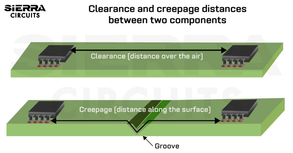
What are creepage and clearance distances?
Creepage is the shortest distance between conductor traces on a PCB measured along the surface of the insulating material. Clearance is the minimum through-air distance (line of sight) between two conductors.

Unlike clearance, which is measured in air, creepage is measured along the surface of the insulation material. While dealing with high-voltage designs, designers need to know the difference between creepage and clearance rules.
What is the significance of creepage and clearance in power electronics?
Creepage and clearance distances are critical in power electronics because they prevent arcing and flashover in high-voltage, high-current systems. This is especially important when the voltage between conductors exceeds the breakdown voltage of the dielectric material.
They are essential for ensuring the safety and reliability of electronic systems, especially in high-voltage applications (above 30 VAC or 60 VDC).
Factors that impact the calculation of creepage and clearance include the working voltage, CTI value, pollution degree (dust and condensation on the board), the type of circuit being assessed, and altitude.
What is the impact of contamination on a circuit board surface?
The trace gets stemmed due to contamination of dust particles and moisture, resulting in current leakage from one or two conductors. This can cause a slow breakdown of the surface of the insulating material between the conductors. The breakdown of the surface may be caused by a voltage spike. The constant high voltage whose comparative tracking index (CTI) is too low will lead to a breakdown of the surface.

6 factors to consider for calculating PCB creepage and clearance
The clearance measurement depends on factors such as the applied voltage, air pollution, and temperature variations. Additionally, humidity decides the breakdown voltage of air and affects the likelihood of arcing. On the other hand, along with board material and environmental conditions, moisture and contamination due to particulate accumulation shorten the creepage distance.

Several factors affecting creepage and clearance include:
1. Comparative tracking index (CTI) of the dielectric material
Comparative tracking index (CTI) defines the electrical voltage breakdown of the insulation material of PCB caused by environmental conditions such as dirt and moisture. It indicates the ability of the PCB substrate to withstand any breakdown between two tracks on the PCB surface. It is used to assess the proportionate resistance of the PCB base material and helps calculate the high-voltage isolation values between the tracks.
The CTI value indicates how resistant the PCB material is against environmental influences such as dirt and moisture. The higher the CTI value of the material, the more resistant it becomes to a breakdown. The default CTI value for FR4 is 175 and goes up to 600 on special materials.
As per the IEC-60112 standard, a higher CTI-grade substrate offers good resistance to electrical breakdown. CTI is a critical number when selecting a PCB material.
The table below defines comparative tracking index values for PCB material selection. IEC has prescribed three of the following classes for PCB CTI calculation:
| Comparative tracking index (CTI) in Volts | Class |
|---|---|
| 600 ≤ CTI | I |
| 400 ≤ CTI < 600 | II |
| 175 ≤ CTI < 400 | IIIa |
| 100 ≤ CTI < 175 | IIIb |
CTI measures the susceptibility of the PCB’s insulating material to electrical breakdown. CTI is that voltage, which results in failure by breakdown after 50 drops of 0.1 percent ammonium chloride solution have fallen on the material.
Depending upon the CTI value of the PCB base material, the creepage value will differ. If the CTI value is higher, then the minimum creepage value is required. In short, a high CTI value indicates a smaller distance between the PCB conductors.
PCB material selection is the first step in the design process. The type of materials you choose defines the quality of your end product. Download our PCB Material Design Guide to learn the art of choosing the right dielectric materials for your design.

PCB Material Design Guide
9 Chapters - 30 Pages - 40 Minute ReadWhat's Inside:
- Basic properties of the dielectric material to be considered
- Signal loss in PCB substrates
- Copper foil selection
- Key considerations for choosing PCB materials
Download Now
2. Working voltage of your circuit board design
A working voltage is the highest voltage across any particular insulation when the equipment is subjected to a rated voltage. This definition is stated in various international standards, including IEC 950 and EN 60950. The creepage and clearance values are calculated by determining the working voltage under a certain operating voltage. While determining working voltages, we need to evaluate both peak and root-mean-square (RMS) voltages. The peak value of the DC voltage will determine the clearance, and the RMS value of the AC voltage will determine the creepage distance.
Based on the working voltage, we calculate the minimum PCB line spacing. For instance, the working voltage of the 609V secondary circuit will withstand the peak voltage of 2700V as per IEC-60950-1, so the root-mean-square (RMS) voltage will be 2700V*√2= 3818V. As per UL 796, the 40V/mil criterion is applied to calculate the required minimum distance. So, the spacing between the two traces would be 3818/40=95.45 mils.
The table below shows how peak-to-peak voltage values vary with working voltages as per IEC-60950-1.
| Working Voltage V(a) | Peak-to-Peak Voltage V(p) |
|---|---|
| 500 V | 1750 V |
| 526 V | 2000 V |
| 551 V | 2200 V |
| 575 V | 2400 V |
| 609 V | 2700 V |
| 620 V | 2800 V |
3. Pollution degree
Pollution degree considers how pollutants will affect products exposed to different environments from a high-voltage/safety standpoint. It is a classification based on the amount of dry pollution and condensation in the surroundings. The higher the pollution degree, the higher the dust contamination and condensation, thus affecting the product’s safety. The creepage and clearance distances are adjusted to ensure the safety of a PCB. The pollution degree varies as per the contamination level and humidity level in the atmosphere.
For instance, laboratory areas come under pollution degree 2 per several safety standards and certification bodies. Pollution degree 1 can be applied to the products that are sealed inside air and watertight enclosures. On the other hand, pollution degree 3 applies to harsh environmental conditions such as industrial manufacturing.
According to the IEC 60947-1 standard, the pollution degree is divided into four major categories:
- Pollution degree 1: Zero pollution or dry environment. In this type, there is non-conductive pollution, which is not harmful to electronic circuit operations. Examples can be sealed enclosures or potted products.
- Pollution degree 2: Mostly, there is non-conductive pollution. However, there is a possibility of temporary conductive pollution, which is caused by condensation. The laboratory area is one of the examples of pollution degree 2.
- Pollution degree 3: In this type, conductive pollution or contamination occurs due to humidity or dust in the surroundings. For example, heavy industrial environments are more exposed to dust.
- Pollution degree 4: There is persistent conductivity, which is caused by the excess of humidity and dust contamination. External conditions, such as rain or snowfall, can lead to pollution degree 4 and result in persistent conductivity.
Controlling the pollution degree with design features
Several steps are taken to avoid the effect of the pollution degree on creepage and clearance. These steps are taken according to the design features related to the PCB line spacing and the operating characteristics of the system.
For instance:
- Pollution degree 1 can be avoided by the hermetic sealing of the product.
- Pollution degree 2 is avoided by limiting the accumulation of humidity or dust particles via ventilation.
- Pollution degree 3 is avoided by using the appropriate enclosures. These enclosures limit external environmental factors such as moisture.
4. Insulation against hazardous voltage
Typically, a single level of insulation is preferred for the electronic circuits that are not accessible. However, we prefer the use of double-level insulation for protection against hazardous voltage. Several rules must be followed to implement a double-level insulation system.
The insulation barriers are necessary for circuits under Safety extra-low voltage (SELV) standards. User-touchable voltage or SELV systems are termed electrical systems in which the voltage cannot exceed a permissible value under normal conditions per IEC and EN 60335 standards. These SELV voltages must be non-hazardous. These SELV circuits operate at low power and logic levels, such as ±3.3 to ±24VDC. Some examples of SELV circuits include input/output connectors and cables attached to peripheral devices such as printers and keyboards.
Classification of insulation types
Insulation types are mainly categorized into five different types, which are functional (F), basic (B), double (D), supplementary (S), and reinforced (R). Definitions for these insulation types are mentioned in multiple standards and are quite complex. You need to know all these rules and apply them in the design as required.
It is highly critical to insulate hazardous voltages from safety extra-low voltage (SELV) circuits. The following insulation types are defined as per international standards:
- Functional insulation: This type of insulation ensures the proper functionality of the product, but it does not guarantee safety protection.
- Basic insulation: This provides a single layer of insulation to avoid any harm to the electronic component.
- Supplementary insulation: This type of insulation adds an extra layer of protection (minimum thickness of 0.4mm) to the basic insulation to protect it from condensation.
- Double insulation: This is a combination of functional, basic, and supplementary insulation.
- Reinforced insulation: This comes under a single system that provides the same protection as double insulation. It also requires a minimum thickness of 0.4mm for use in a single layer (according to UL60950/EN60950).
These safety standards help designers protect the electronic circuit from an abnormal (single-fault) condition. Single-fault conditions are avoided by implementing double or reinforced insulation, where a second layer remains for protection.
Conductive anodic filament (CAF) failure
A conductive anodic filament is a metal filament caused by the electromigration of copper in a printed circuit board. This further leads to device failure. The growth of CAF bridges two oppositely polarised copper conductors.
CAF occurs in four ways: through-hole to through-hole, line-to-line, through-hole to the line, and layer-to-layer. It majorly takes place due to two key factors: a test or bias voltage (voltage applied during the testing of the device) and high relative humidity. CAF failure particularly occurs in the hole-to-hole, as showcased in the diagram below.

The key factors influencing CAF growth include electric field strength, temperature rise, humidity, and the laminate type. CAF failure primarily arises in high-density circuit boards, leading to reduced PCB line spacing. Nevertheless, manufacturing defects can also lead to CAF failure.
The growth of the metal filament is typically from a copper anode to a copper cathode, which ultimately leads to the electrical failure of the electronic circuit. CAF occurs in two stages: the degradation of the resin glass interface and an electrochemical migration of copper, causing filament growth.
The degradation of the resin glass interface is a reversible process where the material’s insulation resistance is restored after the baking and drying processes. The second step of actual CAF growth is believed to be irreversible. The time required for CAF failure to occur depends on test voltage, relative humidity, spacing, temperature rise, and the resin system.
The degradation of the resin glass interface takes place as the PCB behaves like a cell, with the occurrence of the following reaction:
At the anode:
Cu -> Cu(n+) + ne(-)
H2O-> ½ O2 + 2 H+2e(+)
At the cathode:
H2O+ e- -> ½ H2 +2 OH(+)
5. Type of your circuit
To define circuit type, it is essential to identify each circuit block according to SELV (non-hazardous circuits are classified as SELV), ELV, hazardous, etc. This information can be used to define the appropriate insulation type and number of levels for use between circuit blocks and between internal components and the user.
The following categories are used to define different circuit types, along with the type of insulation required:
- Class 0 circuit: Appliances with a class 0 circuit have no protective-earth connection. They feature a single level of insulation. Such appliances are intended for use in dry areas, and a single fault could cause an electric shock. These appliances have been banned in most EU countries.
- Class 01 equipment: They are similar to Class 0, but have an earth terminal, which is unused since two core cables are used.
- Class I equipment: They use protective earthing (e.g., grounded metal enclosure) as one level of insulation; thus, they require only basic insulation between the enclosure and any part of hazardous voltage.
- Class II equipment: They use double or reinforced insulation to eliminate the need for a grounded metal enclosure and a grounded power plug.
- Class III equipment: Powered from a SELV source and without the potential for generating hazardous voltages internally, and therefore only requires functional insulation.
6. Altitude of the system
Environmental conditions, such as altitude, will also influence minimum creepage and clearance distances. As altitude rises, air density decreases, leading to a proportional reduction in airflow. This, in turn, reduces the heat dissipation capacity.
According to Paschen’s law, the dielectric properties of air vary with altitude. When the pressure decreases, the breakdown voltage also decreases. Hence, you must consider this while calculating creepage and clearance distances for high-altitude applications.
The graph below demonstrates how the breakdown voltage varies with the distance between conductors and altitude. It illustrates how the breakdown voltages change with pressure (altitude) and temperature (inversely proportional).

Breakdown voltages vary with the altitude. For a 1 cm space between conductors at sea level, it is 30 kVdc. At 50000 feet, it drops to 1.2 kV, and at 150,000 feet, it further decreases to 300V.
At higher altitudes ranging from 2,000 to 5,000 meters above sea level, the reduced air pressure leads to increased peak overvoltages. These surges result in arcing between isolator pins.
To ensure consistent safety measures against electrical breakdown at higher altitudes, it is necessary to enhance both clearance and creepage distances. The increased distance needed is directly related to the decrease in air density. IEC 60664-1 offers precise guidelines for clearance requirements (>2000 m above sea level operation). It provides multiplication factors to calculate safe clearance distances to avoid arcing caused by high altitudes.
Table A.2 of IEC 60664-1:2007 provides correction factors for altitudes exceeding 2000 m.
| Altitude | Multiplication Factor for Clearance |
|---|---|
| 2000 | 1 |
| 3000 | 1.14 |
| 4000 | 1.29 |
| 5000 | 1.48 |
| 6000 | 1.7 |
| 7000 | 1.19 |
Design guidelines to avoid PCB creepage and clearance issues
Lower clearance leads to over-voltage, resulting in an instantaneous fault between neighboring conductive traces. Adopt the following measures to resolve clearance and creepage issues:
- Have sufficient spacing between high voltage and low voltage circuits as per the standard.
- Bend the traces using curves rather than any angle.
- Select board material with high dielectric breakdown and high CTI. Always consult your CM before finalizing the material.
- Apply conformal coating to protect your board from external contamination; however, its composition is dielectric, which adds insulation to your PCBA surface.
- Add a slot between traces or place vertical insulation barriers. Incorporating a V-groove, parallel-sided notch, or placing a slot in your design can solve creepage issues.
We know that creepage is the space between PCB conductors along its surface. We need to maintain both a minimum creepage distance and packing density at the same time. Let us discuss some techniques that will help increase packing density while maintaining the desired creepage distance.

- Default situation of a flat insulating surface: In this method, the creepage is measured along the PCB surface between two conductors. You can increase the creepage distance by increasing the distances between the traces.
- V-groove method: In this scenario, the V-groove increases the surface distance between the conductors. The increased surface length is measured down to the groove until it reaches at least 1mm or more.
- Parallel-sided notch approach: It further increases the surface distance, but should be at least 1mm or more wide.
- Slot implementation: A slot with a width of over 1mm can further increase the creepage distance. This method is one of the easiest and most cost-effective methods. However, it has one limitation: it requires free space, which is why it cannot be applied all the time.
Sierra Circuits fabricates and assembles high-quality circuit boards in the United States. Visit our PCB manufacturing capabilities to learn more.
What type of materials and components are required for high-voltage PCB designs?
High-voltage PCB designs require materials and components with strong dielectric strength, high insulation reliability, and adequate current-carrying capability to safely withstand continuous operating voltages and overvoltage events.
Designers need to keep the following points in mind:
- Components: Select components that can handle high operating voltages. Make sure sufficient spacing is maintained between the terminals. Follow the layout guidelines mentioned in the component datasheet.
- Board material: Select PCB laminates with very high dielectric breakdown. High-voltage laminates have very high performance and high prices.
- Copper: The copper used to create PCB traces and vias should have a thickness of 2 to 3 Oz. to withstand high currents and mechanical stress.
- Resin and glass: The resin and glass levels on board influence its durability in high-voltage situations. A board with high resin content and a small glass style offers the best dielectric properties.
What standards define PCB creepage and clearance requirements?
Benchmarks such as IPC-2221, IEC 62368-1, and UL 61010-1 define the minimum spacing requirements needed to prevent electrical breakdown, maintain insulation integrity, and ensure safe operation in high-voltage designs. As voltage increases, separation requirements generally become more stringent. The required values depend on operating voltage, pollution degree, insulation type, conformal coating, and installation altitude.
Selecting the correct creepage and clearance is essential for safe operation and long-term reliability. Insufficient spacing can lead to flashover, insulation failure, regulatory non-compliance, or equipment damage.
The following sections explain the key standards used to determine spacing requirements.
IPC-2221 generic standard on printed board design
IPC-2221 is the generic standard for guidance on PCB creepage and clearance. This standard explains in detail the requirements for material quality, traceability, and layout guidelines to ensure quality. If you are following the IPC-2221A rule set, you can assume that adequate isolation has been provided. A high-voltage clearance calculator based on IPC-2221 is very helpful in determining the minimum spacing for your PCB. For the IPC 2221 standard, calculators are also available for creepage and clearance measurements.
The table below shows the optimum conducting spacing requirements as per the IPC-2221B standard:
| Voltage (ACV or DVC) | B1 (mm) | B2 (mm) | B3 (mm) | B4 (mm) | A5 (mm) | A6 (mm) | A7 (mm) |
|---|---|---|---|---|---|---|---|
| 0-15 | 0.05 | 0.1 | 0.1 | 0.05 | 0.13 | 0.13 | 0.13 |
| 16-30 | 0.05 | 0.1 | 0.1 | 0.05 | 0.13 | 0.25 | 0.13 |
| 31-50 | 0.1 | 0.6 | 0.6 | 0.13 | 0.13 | 0.4 | 0.13 |
| 51-100 | 0.1 | 0.6 | 1.5 | 0.13 | 0.13 | 0.5 | 0.13 |
| 101-150 | 0.2 | 0.6 | 3.2 | 0.4 | 0.4 | 0.8 | 0.4 |
| 151-170 | 0.2 | 1.25 | 3.2 | 0.4 | 0.4 | 0.8 | 0.4 |
| 171-250 | 0.2 | 1.25 | 6.4 | 0.4 | 0.4 | 0.8 | 0.4 |
| 251-300 | 0.2 | 1.25 | 12.5 | 0.4 | 0.4 | 0.8 | 0.8 |
| 301-500 | 0.25 | 2.5 | 12.5 | 0.8 | 0.8 | 1.5 | 0.8 |
| >500 | 0.0025 mm/volt | 0.005 mm/volt | 0.025 mm/volt | 0.00305 mm/volt | 0.00305 mm/volt | 0.00305 mm/volt | 0.00305 mm/volt |
Where:
B1 internal conductors.
B2 uncoated external conductors, up to an altitude of 3050 meters above sea level.
B3 uncoated external conductors, exceeding an altitude of 3050 meters above sea level.
B4 polymer-coated external conductors at any altitude.
A5 conformal-coated external conductors at any altitude.
A6 uncoated external component leads/terminations up to an altitude of 3050 meters above sea level.
A7 conformal-coated external component lead termination at any altitude.
IEC 62368
IEC 62368-1 is a safety standard that identifies energy sources and outlines safety measures against them. The following table illustrates the creepage requirements for electronic systems, especially for high-voltage applications.
| Creepage requirements in electronic circuits (mm) | |||||||
|---|---|---|---|---|---|---|---|
| RMS working voltage | Pollution degree- 1 | Pollution degree-2 | Pollution degree-3 | ||||
| Material group I, II, IIIa, IIIb | Material group I | Material group II | Material group IIIa, IIIb | Material group I | Material group II | Material group IIIa, IIIb |
|
| 25 | 0.125 | 0.500 | 0.500 | 0.500 | 1.250 | 1.250 | 1.250 |
| 32 | 0.14 | 0.53 | 0.53 | 0.53 | 1.30 | 1.30 | 1.30 |
| 40 | 0.16 | 0.56 | 0.8 | 1.1 | 1.4 | 1.6 | 1.8 |
| 50 | 0.18 | 0.6 | 0.85 | 1.2 | 1.5 | 1.7 | 1.9 |
| 63 | 0.2 | 0.63 | 0.9 | 1.25 | 1.6 | 1.8 | 20 |
| 80 | 0.22 | 0.67 | 0.95 | 1.3 | 1.7 | 1.9 | 2.2 |
| 100 | 0.25 | 0.71 | 1 | 1.4 | 1.8 | 2 | 2.2 |
| 125 | 0.28 | 0.75 | 1.05 | 1.5 | 1.9 | 2.1 | 2.4 |
| 160 | 0.32 | 0.8 | 1.1 | 1.6 | 2.0 | 2.2 | 2.5 |
| 200 | 0.42 | 1.0 | 1.4 | 2 | 2.5 | 2.8 | 3.2 |
| 250 | 0.56 | 1.25 | 1.8 | 2.5 | 3.2 | 3.6 | 4 |
| 320 | 0.75 | 1.6 | 2.2 | 3.2 | 4 | 4.5 | 5 |
| 400 | 1 | 2 | 2.8 | 4 | 5 | 5.6 | 6.3 |
| 500 | 1.3 | 2.5 | 3.6 | 5 | 6.3 | 7.1 | 8 |
| 630 | 1.8 | 3.2 | 4.5 | 6.3 | 8 | 9 | 10 |
| 800 | 2.4 | 4 | 5.6 | 8 | 10 | 11 | 12.5 |
| 1000 | 3.2 | 5 | 7.1 | 10 | 12.5 | 14 | 16 |
IEC-60950-1 (2nd edition)
IEC-60950 is another important standard that describes spacing in IT & Telecommunication products with AC main or battery power supply, especially if you want to sell those products internationally. This standard safeguards values regarding pollution degrees, insulation types, and isolation distances.
UL61010-1: Electrical equipment for laboratory use
The table below lists the standards for electrical safety and isolation in high-voltage applications.
| Organization | |||||
|---|---|---|---|---|---|
| International | Europe | U.S. | Canada | Germany | |
| Application | IEC | CENELEC (EN) | UL | CSA | DIN/VDE |
| Industrial | 204 604 | 50178 | 508 | 14-M91 | 160 |
| IT equipment | 950 | 60950 | 60950 | 950 | 60950 |
| Medical equipment | 601 | 60601 | 2601-1 | 601 | 750 |
| Household | 65 | 60065 | 8730-1 | 860 | |
| Measurement and control | 1010-1 | 61010-1 | 1262 | 1010 | 0410 0411 |
| Telecom | 950 | 60950 | 1459 | 225 | 804 |
Key takeaways:
- PCB line spacing is crucial for product safety when operating voltages that exceed 30VAC or 60VDC, as it can lead to electrical arcing and PCB failure.
- Adhere to safety guidelines such as IPC 2221A and UL 60950-1 when designing circuit boards with high voltage.
- Higher CTI values indicate better resistance to breakdown. Furthermore, it also indicates a smaller distance between PCB conductors, necessitating a minimum creepage value.
- Working voltage, pollution degree, insulation, altitude, circuit type, and environmental conditions influence creepage and clearance.
- To control pollution degrees, include design features such as hermetic sealing, ventilation, heaters and fans, continuous energizing, and appropriate enclosures.
- Insulation types such as functional, basic, supplementary, double, and reinforced protect circuits from abnormal single-fault conditions.
- Altitude influences creepage and clearance distances due to variations in air density and dielectric properties of air. Apply the correction factor specified in IEC 60664-1 for altitudes above 2000 meters to avoid arcing caused by high altitudes.
Need help in designing reliable PCBs? Our engineers can help you with material selection, stack-up design, layout planning, and DFM analysis.
You can book a meeting with our experts or call us at +1 (800) 763-7503.

As a PCB designer, you need to calculate the creepage and clearance distances carefully. Consult product safety engineers during the design stage to avoid any failure at the test house before launching a product into the market. It is also important to note that as working voltage, pollution degree, overvoltage category, and altitude increase, the creepage and clearance distances also increase.
Need assistance in designing your high-voltage circuit boards? Post your queries on our PCB forum, SierraConnect. Our design and manufacturing experts will resolve them.

About Mohamed Faheemuddin : Mohamed Faheemuddin is a mechanical engineer. His passion for electronics drew him to the PCB industry. With an experience of over 3 years in the PCB industry, he specializes in developing articles for engineers and hardware designers.


Start the discussion at sierraconnect.protoexpress.com