


Contents
Building a multilayer PCB stack-up involves defining the layer arrangement, selecting appropriate materials, and structuring power, ground, and signal layers to meet electrical and manufacturing requirements.
When designing these build-ups, layout engineers must carefully plan for routing density, controlled impedance, and reliable power distribution across the board.
In this article, you’ll learn what a stack-up is, the layers involved in a multilayer board, how these boards are manufactured, and the key guidelines for designing reliable and high-performance boards.
Highlights:
- Define an optimal layer stack-up to support complex routing and signal integrity.
- Select appropriate materials, copper thickness, and dielectric properties.
- Use power and ground planes for stable voltage distribution and reduced EMI.
- Follow proper manufacturing processes to ensure reliability and performance.
What is a PCB stack-up?
It describes the construction of a multilayer board in sequential order. A layer stack provides vital information like material thickness and copper weights required to fabricate a printed board. They are also referred to as build-ups.

A stack-up also gives the details of trace width for different controlled impedance traces, such as 50 ohms or 100 ohms differential.

What are the different layers present in a circuit board?
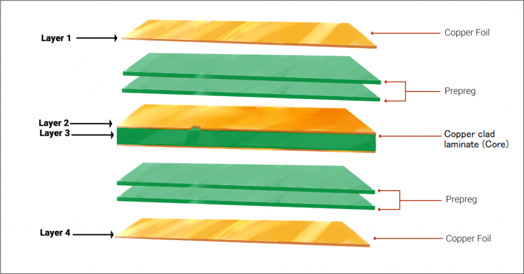
A PCB build-up primarily consists of metal foil, prepreg, and copper-clad laminate (core).

- Metal foil: Copper is the most commonly used metal foil in board construction.
- Prepreg: It is an interwoven glass cloth impregnated with epoxy resin. The resin is left semi-cured.

- Copper-clad laminate: Single or multiple plies of prepreg bonded together, along with the top and bottom copper foil, make a copper-clad laminate. This is also known as the core.
What are power and ground planes?
The power plane is a copper layer connected to the supply of the board. It is often designated as VCC. The ground plane is a copper layer connected to the common ground point of the printed board.
The main function of the power plane is to provide a steady voltage supply to the circuit board. In multi-layered boards, if a component needs to draw power, then it is simply connected to the via that makes contact with the power plane.
Advantages of using power/ground planes
- The power and ground pins of the components can easily be connected to the power and ground planes.
- It provides a clear current return path, especially for high-speed signals, which reduces EMI (electromagnetic interference).
- The power planes have a larger current-carrying capacity than the traces, which reduces the PCB’s operating temperature.
What is PCB lamination?
It is the process of placing the stack-up under extreme temperature and pressure to bond prepreg and copper foil to the base inner layers. The temperature and pressure values are mentioned in the datasheets of the chosen board materials.

For more, download the PCB Stack-up Design Guide.
PCB Stack-Up Design Guide
12 Chapters - 55 Pages - 60 Minute ReadWhat's Inside:
- Design guidelines for HDI, flex, and hybrid stack-ups
- Stack-up representation in fab drawing
- DFM checks for layer stacks
- Characteristics of high-speed materials
- Manufacturing tolerances
- PCB stack-up examples with illustrations
Download Now
What is the standard board thickness?
The typical thickness of a conventional board is around 62 mil (1.57mm).
It mainly depends on factors such as copper thickness, materials used, number of layers, and the operating environment.
Today, PCBs have become more complex as the copper layer weight and the layer count have increased for various applications.
Due to this, the printed boards tend to become thicker. Manufacturers, based on the customer’s request, are now fabricating boards with two new standard thicknesses, 93 mil (2.36mm) and 125 mil (3.17mm) (150% and 200% of the old standard thickness).
Need printed boards? Talk to a PCB expert: Book a meeting or call us at +1 (800) 763-7503.
Why do we need multiple layers in a PCB?
Multiple layers in a printed circuit are required to accommodate complex circuits, improve electrical performance, and optimize space utilization.
As electronic devices become more sophisticated, the number of components and interconnections increases, making it impractical to route everything on a single-layer board. Adding layers allows designers to efficiently manage dense routing, incorporate dedicated power and ground planes, and maintain signal integrity.
Let us have a look at a few advantages of a multilayer PCB stack-up:
- They are capable of accommodating complex circuits that are required for modern electronic devices.
- Having more layers means the board is thicker and, therefore, more durable than single-sided printed circuit boards.
- Multi-layer boards require more planning and intensive production processes, so they are of a higher quality than other types of boards.
- Using multiple circuit board components would require multiple connection points. Multi-layer boards, on the other hand, are designed to work with a single connection point, simplifying the design of the electronic device and further reducing the weight.
How are multilayer circuit boards made?
Multilayer PCB stack-ups are manufactured by sequentially preparing patterned inner layers, accurately stacking them with insulating materials, and bonding them under heat and pressure to form a single integrated structure with electrical interconnections between layers.
The steps involved are explained in detail below:
Step 1: Inner layer core selection

The build-up designates the materials to be used for the manufacture of a multilayer circuit board. The build-up provides the following information:
- The copper thickness and weight
- Type of epoxy glass to be used
- Panel size
Step 2: Cleaning
The inner layers are cleaned chemically/mechanically or both to remove contaminants from the copper surface.
Step 3: Inner layer imaging

The imaging material is placed on the copper surface. It covers the desired copper circuitry and exposes the unwanted copper.
Step 4: Etch stripping
The inner layers are chemically etched to get rid of the unwanted copper. The photoresist is then stripped off to reveal the copper circuitry.
Step 5: Automated optical inspection
Automated optical inspection is carried out to find the flaws(shorts/opens in inner layers) that can’t be detected by the human eye.
Step 6: Oxide treatment

The exposed copper circuitry on the inner layer must be treated before lamination to improve adhesion. Improved adhesion also increases the structural strength and overall board reliability.
Step 7: Layup
Steps 1 to 6 are repeated for all the inner layers. For example, these steps will be carried out for layers 2, 3, 4, and 5.
Step 8: Lamination

In this step, the stacks are pressed and heated in a vacuum chamber. The lamination process begins by applying a vacuum to remove all the entrapped air and gases. Later, heat and pressure are applied to the stack so the resin in the prepreg undergoes molecular bonding. Check out our article to learn about the causes of lamination voids.
Step 9: Drilling
After the lamination process, the laminated board is loaded on a panel of exit material on the drill bed. The holes are drilled on the board to make vias and through holes.
The exit material lessens the burr formation. Burr is the protruding part of copper formed when the drill spindle penetrates through the board. To learn more about drilling, check out our article PCB Drilling Explained: The Do’s and the Don’ts.
Step 10: Deburring and desmearing
In this step, the copper burrs formed during the drilling process are removed. It also removes any fingerprints on the copper surface. Desmearing is the process of removing friction-melted resin during the drilling process.
The epoxy smear is removed by immersing the circuit board panel in a series of chemical solutions, followed by potassium permanganate or concentrated sulfuric acid. Desmearing can also be performed by plasma treatment.
Step 11: Copper plating of drill holes
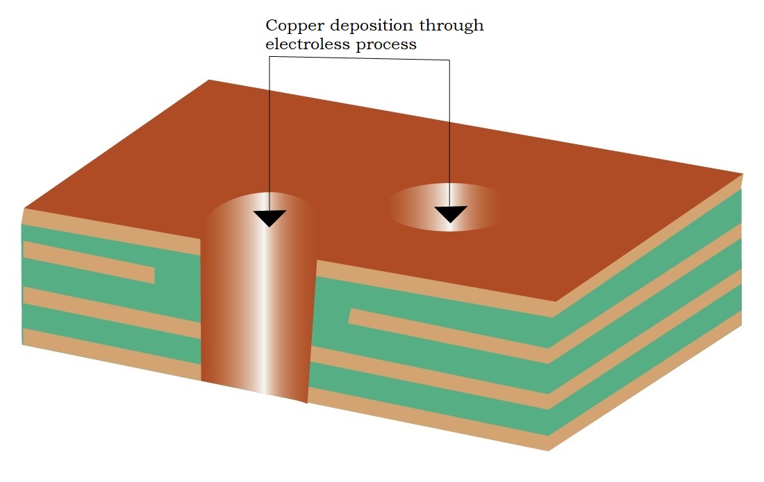
After deburring and desmearing, drill holes are copper-plated using an electroless method.
What are HDI board stack-ups?
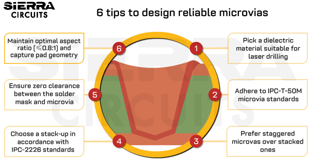
HDI board stack-ups are multilayer configurations designed to achieve high routing density by using advanced features such as microvias, blind and buried vias, and sequential lamination. These build-ups enable compact layouts, improved signal performance, and efficient interconnection of densely packed components.
For high-density layout strategies, download the HDI PCB Design Guide.

HDI PCB Design Guide
5 Chapters - 52 Pages - 60 Minute ReadWhat's Inside:
- Planning your stack-up and microvia structure
- Choosing the right materials
- Signal integrity and controlled impedance in HDI
- Manufacturing considerations for higher yields
Download Now
What is sequential lamination?
Sequential lamination is a process in which layers are built and laminated in multiple stages by inserting a dielectric between a copper layer and a laminated subset (laminated layers).
PCBs are manufactured by layering an epoxy pre-impregnated fiberglass sheet between the copper layers. These layers are laminated together under high temperatures and pressure.

Buried vias can be built into HDI boards using a sequential lamination process. The first step is to fabricate the layers that are connected through a buried via (layers 2, 3, 4, and 5 in the given build-up). Next, the outer layers (layers 1 and 6) are laminated, and the microvia holes are drilled.
Now, let us assume that this design requires a connection between L1 & L3; L6 & L4. The best way to achieve this design is to use staggered or stacked vias as shown below.

In the image above, we can see that the micro-vias are stacked and staggered. Stacked vias are more space-efficient. However, they are less reliable and require complex manufacturing, which increases the manufacturing price.
Staggered vias essentially mean fewer process steps. We do not have to fill the laser-drilled vias with copper because the second laser drill does not land on the first laser drill. Filling or plating a microvia shut usually happens in a special plating tank designed with chemistry.
It plates the laser-drilled microvia from the bottom of the via to the top of the via until it fills the hole completely. Plating a laser-drilled microvia shut adds time and cost to the process.
Nomenclature of HDI stack-ups
HDI layer stacks are named using the X–N–X nomenclature, where X represents the number of microvia layers, and N denotes the number of core (inner) layers between them. This naming convention helps define the complexity of the high-density structure based on via layering and build-up design.

Sierra Circuits utilizes self-learning automated scaling software (XACT) to ensure precision in HDI build-up design. The system analyzes material type, thickness, and copper weight on each layer to accurately predict and compensate for material shrinkage.
To learn more, see HDI PCB capabilities to learn more.
Examples of HDI build-up
1+4+1

The above image shows an example of a 6-layer stack-up (1+4+1) with one microvia layer on either side of the board.
2+4(6b)+2
+2 HDI stack-up")
The above image shows an example of an 8-layer build-up with two microvia layers on either side of the board and 6 buried via layers between the microvia layers.
PCB stack-up recommendations for designers
The cost of a board needs to be optimized as low as possible. To achieve this, the following points need to be considered:
- Limit the number of sequential lamination layers to three or fewer, as each additional layer increases processing time, cost, and delivery schedule.
- Avoid stacked vias when possible, since they require filling after each sequential layer and add extra manufacturing steps and time. Use staggered vias instead.
- Clearly specify the required build-up details to the manufacturer, including the layers between which mechanical buried vias are needed and whether staggered or stacked vias are required.
- Verify that the selected materials are suitable for sequential lamination by consulting with the manufacturer.
A successful board design relies heavily on the build-up. A well-designed multilayer PCB stack-up enables designers to optimize their designs for better signal integrity and reduced crosstalk and EMI.
Need assistance designing your PCB? Post your queries on our forum, SierraConnect. Our design and manufacturing experts will help you select one.

About Milan Yogendrappa : Milan Y is an electronics and communication engineer with over 6 years of experience in developing and editing technical articles related to PCB design, manufacturing, and assembly. He is currently the editor-in-chief at Sierra Circuits.


Start the discussion at sierraconnect.protoexpress.com