


Contents

On-demand webinar
How Good is My Shield? An Introduction to Transfer Impedance and Shielding Effectiveness
by Karen Burnham
A PCB schematic is designed by creating a clear and accurate representation of the electrical connections between components. To ensure an error-free circuit diagram, engineers must clearly label the nets, organize the signal flow, use standardized symbols, and perform design rule checks.
In this article, you’ll learn the best practices for creating a reliable PCB schematic for your design.
Highlights:
- Implement efficient net labeling, off-page connectors, and signal flow representation to improve schematic readability.
- Create standardized component symbols, assign reference designators, and generate accurate BOMs.
- Run ERC checks, verify netlists, and maintain revision history to minimize schematic design errors.
What is the importance of a schematic diagram?
A PCB schematic illustrates the electrical connections between various electronic components. It helps you understand the overall circuit functionality.
A technically correct but crowded circuit diagram is still a bad one, as it might confuse you. Schematics can also be an extremely valuable troubleshooting tool during circuit board repair.
How to draw a PCB schematic diagram?
A schematic diagram is designed by following standard design practices that ensure clear signal flow, accurate component representation, easy readability, and error-free connectivity.
Follow the guidelines below:
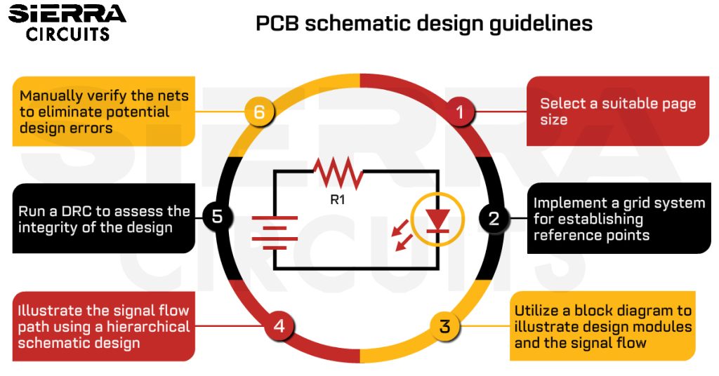
1. Select a suitable page size
Most design tools offer multiple page sizes, with A4 selected as the default size. Various page sizes are available. However, the page size should be selected based on the size and complexity of the circuit design.
2. Name the pages in alphabetical order
The logical blocks of the schematic should be separated by pages. The pages can be named using the letters A, B, C, and so on. By doing this, we can place the pages in alphabetical order. An example of such a naming convention is shown below.
- A_Block Diagram
- B_Power supply
- C_ MCU interface
- D_Memory interface
- E_ Revision history
Block diagrams and revision history are often ignored by most designers to save time. However, they can be very helpful for other designers trying to understand the schematic. Product-based organizations mandate all such protocols and regulations.
3. Implement a grid system for establishing reference points
A grid system helps define reference points for components and connections in the PCB schematic. Keeping circuit components and connections placed on the grid improves part referencing and simplifies net probing during analysis.
4. Include a title block in the footer of the page
The page title block is present in the footer of the schematic page. It should consist of all the required details, such as page size, update date, revision, document number, name/function of the circuit, and company disclaimer. An example of the title block is shown below.

5. Add important notes/comments on separate pages
Important comments related to the circuitry should be documented clearly. These notes can be added either on schematic pages or in separate documents. For complex designs, notes are generally included on separate pages. Examples of notes could include jumper status and PCB layout constraints/guidelines. A schematic with notes can be seen below.

6. Include a revision history on the first or last page
The revision history contains the changes that were made to the design. This document provides information such as the date and description of the changes made, the name of the author and the reviewer, and review comments, if any. Revision history is generally placed on the first or last page of the schematic. An example of PCB schematic revision history is shown below.

7. Incorporate a table of contents into the schematic document for easy navigation
The table of contents lists the topics present in the schematic document. This page helps you easily locate a specific module in a complex and large design. This can be skipped if the design is small and simple. An example of a ToC is given below.

8. Utilize a block diagram to illustrate design modules and the signal flow
The block diagram represents the different modules in the design and signal flow. This makes it easy for the reviewer to understand the design for review purposes. Block diagrams may not be required for simpler designs, but are primarily used in more intricate projects. An example of a schematic block diagram can be seen below.

Implement auto-grouping of repetitive PCB design blocks if you have redundant blocks in your layout.

Design for Manufacturing Handbook
11 Chapters - 96 Pages - 90 Minute ReadWhat's Inside:
- Annular rings: avoid drill breakouts
- Vias: optimize your design
- Trace width and space: follow the best practices
- Solder mask and silkscreen: get the must-knows
Download Now
9. Illustrate the signal flow path using a hierarchical schematic design
If the design is complex and contains many modules, a hierarchical design is preferred. The hierarchical schematic clearly displays the signal flow from one module to another, as shown below. A detailed view of each module can be accessed by clicking on the respective module in the hierarchical schematic.

10. Use standard reference designators for schematic components
The table below shows the names of the generally used electronic components and their corresponding reference designators used in any schematic. These designators are assigned according to IEEE standards. It is recommended to name the components with their standard reference designators. Also, always use capital letters to designate the schematic symbols.
| Component | Reference designator | Component | Reference designator | Component | Reference designator |
|---|---|---|---|---|---|
| Resistor | R | Plug /Connector | P/CON | Power supply | PS |
| Capacitor | C | Jumper | Jp | Crystal | X or Y |
| Diode/LED | D | Cable/wire | W | Oscillator | OSC |
| Zener diode | Z | Test Point | Tp | Heatsink | H |
| Resistor Network | Rn | Relay | K | Fiducial | Fd |
| Inductor/Bead | L | Fuse | F | Buzzer/Loudspeaker | LS |
| IC (Integrated Circuit) | U/IC | Switch | SW | Battery | BT |
11. Generate component symbols using the standard library
The PCB schematic diagram consists of different types of components, such as active components, passive components, and connectors. Active components include transistors, diodes, logic gates, processor ICs, FPGAs, Op-amps, and so on.
Components like capacitors, inductors, and transformers are referred to as passive devices. Creating new symbols is not advisable unless the symbol for that component is not present in the standard library.
For more on symbol generation, see how to create a schematic and symbol library in KiCad.
Resistors
Resistors can be represented in two different ways, as shown below. You should take care to keep up the consistency in the symbols used.

The unit of resistance is ohms and is represented by the symbol ‘Ω.’ Sometimes, the symbol ‘Ω’ can be replaced with the letter ‘E’. You should ensure that consistent unit representation is followed throughout the entire design. All required data about the components should be entered in the design tool. This makes it easier to create a BOM at the end of the design.

Polarized and non-polarized capacitors
Capacitors have two terminals, one positive and one negative. Care should be taken to mark the polarity of these terminals. Incorrect capacitor polarity can damage the component and may even cause it to explode during operation. The figure below shows the capacitor symbols from IEEE standards.

You should also ensure that the pin numbers assigned to the symbols match the footprint layout.
Transistors
A transistor is a three-terminal semiconductor device. The terminals are the base, collector, and emitter. You should always refer to the component datasheet while mapping the pins in the footprint layout to the schematic symbol.

When the symbols are created, it is important to enter a description of the component. This is very useful for future reference or when the part is obsolete and needs to be replaced. Having these details on the BOM improves readability. The two images below show filled description fields of a transistor symbol.


Op-amps
It is very important to create the op-amp symbol per the IEEE standards. Many designers often draw the op-amp as per their convenience, which tends to lose readability. This may happen due to a lack of understanding and experience with CAD schematic tools.

When you create a symbol, it is recommended to have all the input pins on the left and all the output pins on the right. Similarly, power and ground pins can be placed at the top and bottom, respectively. In the image shown, the input pins are 2 and 3, the output pin is 4, and the power and ground pins are 7 and 4, respectively.
You should be careful while flipping or changing the orientation of the symbol. When we do so, there is a good chance that positive and negative terminals will switch their positions.
Failure to adjust the wiring after flipping symbols can lead to misalignments between the schematic and physical connections, potentially causing incorrect functionality or circuit failure. Hence, care should be taken to cross-check each symbol with the manufacturer’s datasheet.
Heterogeneous schematic symbol
Complex devices such as FPGAs, memories, and microprocessors are called heterogeneous components. These components have different types of pins in large numbers, such as data lines, inputs/outputs, address lines, control lines, and power lines.
To retain clarity and readability, you should create multiple components of a single package, such as UxA, UxB, UxC, and UxD.
Some pins on components may have multiple functions, and this flexibility is usually denoted on the symbol, accompanied by specific details provided outside the symbol. For instance, pin AA5 below is assigned various functions, such as GPIO.6, CLKOK, PWM, or T3.
Additionally, external notes at the connection point specify the current function of the pin; for instance, the label “GPIO6” outside the symbol indicates its present function.
An example of such a heterogeneous schematic symbol of a component is given below.

Power and ground symbols
The symbols of power and ground pins are shown below.

It is always a good idea to represent voltages with a ‘+’ sign since there could be negative voltages present on the board. You should follow a standard and consistent convention to represent the voltage levels and their sections inside the silicon.
For example, +3.3V_IO, +3.3V_DG, +3.3V_AN +1.8V_Core, +1.2V_LVCore, +2.5_Vref etc.
Similarly, different types of grounds could be present on the board. The symbols are shown below.

12. Reduce unnecessary net connections to enhance clarity
Whenever you have two wires that form a junction and share an electrical connection, that intersection needs to have a junction dot. This is a standard practice in every schematic design.
However, most schematic design software applications exclude the junction dot when a wire connects directly to a pin or terminal on a component.

Net labeling conventions
The objective of a circuit diagram is to make your layout easier to understand for you as a designer. Unnecessary connections should be minimized. This is commonly observed when drawing the symbol of an integrated circuit (IC) on a schematic.
Rather than drawing dozens of nets all over the place, you can assign a net name for a specific pin, which is associated with a pin on another device. These pins will have the same name. Pins with the same name are assumed to be connected.
This approach is especially beneficial when the net is linked to three or more locations. The image below shows a series of named nets.

Net labeling guidelines
When nets are connected on the same page directly to another IC, net naming is not required.
You can follow these simple rules while naming the nets:
- Signal names should always be written in uppercase and should be placed just above the net.
- Avoid long names. Preferably, the names can have a maximum of 4 letters.
- Describe active low or high signals using the upper bar. A pin with an upper bar is considered to be an active low pin.
- Open nets/connections should be removed.
Off-page connection
To improve readability, designers usually name the nets in the schematic. This works fine when the signal is to be connected on the same page. If there is a requirement to connect the net to a pin that is present on a different page, an off-page connector symbol should be used.
Signal flow representation
On a schematic page, the signal flows from the left to the right side of the page. Any power and ground connections are shown on the top or bottom side of the page, respectively. You are advised to keep this in mind and to keep components accordingly.
Need help creating error-free PCB schematics? Our design experts can help you build reliable, manufacturing-ready circuit diagrams.
You can book a meeting with our experts or call us at +1 (800) 763-7503.

13. Maintain readability when depicting the component placement
Component placement in a schematic is one of the important tasks. This is because the layout engineer is going to keep the components accordingly. The parallel connection of the capacitors is shown on the left. As we can see, the readability of the schematic is not up to the mark.

To improve the readability, the connection can be made as shown below.

Also, read How to Place Components in KiCad.
14. Place components connected to the crystal in close proximity
Crystal placement in the PCB schematic is always made, as shown below. The components connected to the crystal are always placed near i,t as the signals could be of high frequency.
Typically, when the design requires placing two components in close proximity, they should be illustrated accordingly (e.g., shunt and series terminations).

For more information on high-speed schematic design tips, see how to create a schematic for high-speed designs in KiCad.
15. Run an ERC to assess the integrity of the design
Electrical Rule Check (ERC) is an intelligent feature offered by PCB design software to check both the logical and physical integrity of a design. Checks are made against all enabled design rules and can be made online as you design.
16. Manually verify the nets to eliminate potential design errors
The netlist is generated when the schematic design is complete and ready to be imported into the layout. The most common file extension for a netlist is .net. Manually verifying the nets is recommended to avoid design errors.
For more, read schematic and netlist checks to ensure error-free design.
17. Generate a complete BOM by importing components from the library
Currently, CAD tools provide a key feature called BOM creation. A complete and sufficient BOM can be generated only if you have provided all the inputs in the tools while creating or importing components from the library.
The inputs to the BOM could be MPN (Manufacturing Part Number), package, vendor name, vendor part number, and so on. It is recommended to provide all the required information during the symbol creation.
Checklist for a flawless PCB schematic
The schematic checklist is the most often ignored point in the design phase. This is more related to the organization’s process, which is based on past design experiences.
Below is the checklist.
- Verify pin numbering and labels for each component and align them according to the datasheet.
- Conduct a polarity check for all polarized components.
- Check for overlapping labels and pin numbers to ensure legibility.
- Validate the alignment of the base, collector, and emitter pins of transistors with the datasheet, symbol, and footprint package.
- Confirm the accuracy of component values, reference designators, and physical locations.
- Ensure the presence of symbol descriptions, such as MPN, vendor name, and vendor part number.
- Check the off-page connector presence and its accuracy.
- Verify inter-sheet references for seamless connectivity.
- Conduct checks on decoupling capacitors for all ICs, ensuring proper ground pin separation based on signal type (analog, digital, signal, ground).
- Perform bill of materials checks, including package types, quantity, and part numbers.
A good PCB schematic should ensure a seamless transition from a good concept to a layout. From net labeling to component symbol creation, you need to adhere to the set of standard guidelines to ensure an error-free PCB schematic.
Need assistance in creating schematics for your PCB designs? Post your queries on SierraConnect; our design experts will help you!


