


Contents

On-demand webinar
How Good is My Shield? An Introduction to Transfer Impedance and Shielding Effectiveness
by Karen Burnham
Circuit board manufacturers have invested in advanced modeling software and testing devices to specify the controlled impedance requirements to fulfill the demand surge.
Nowadays, more PCB designs require impedance control and testing than ever before, thanks to the ubiquity of sophisticated processors, USB devices, and antennas printed right onto the board surface.
Board designers should know the best possible way to communicate their expectations to the manufacturers when creating documentation for controlled impedance. Even if it seems small, a piece of missing information can make it difficult or impossible for the fabricators to know exactly what the designer needs.
Controlled impedance affects the combination of material types and their thicknesses a manufacturer needs to implement to meet the target impedance. Any micro-adjustments that may be required to the Gerber files in pre-production also impact the target impedance. If the impedance callouts are unclear, it becomes impossible for the fabricator to plan the order because the bill of material (BOM) of the stack-up is unknown. The order is ultimately kept in pre-production until the missing data is received.
Fortunately, stating the regulated impedance criteria is not difficult. The first step is to figure out which pieces of information will be required so that the order can proceed easily without delays.

Why it is important to specify controlled impedance requirements?
PCB designers usually include callouts for different parameters, such as material types, copper weight, and the number of layers in the documentation. This assists in easily determining the controlled impedance requirements.
Designers generally provide values for a few distinct factors to specify impedance:
- Target impedance
- Trace width
- Trace height
- Layers on which the impedance traces are present
- Spacing between copper components on controlled traces (for coplanar or differential calculations)
If the controlled impedance requirements are very specific, a chart with target impedance values, trace widths, copper weights, and layer thicknesses should be included. A chart assists to clarify any ambiguities using a visual depiction of these requirements.
These are just a few parameters, and some of them may already be included in the PCB documentation. As a result, in certain situations, no additional effort is required to define impedance control. When developing or manufacturing high-layer-count circuit boards, layer stack-up design tools like Instack are advantageous.
After mentioning the controlled impedance requirements, obtain the board stack-up design from the manufacturer.

How to specify controlled impedance requirements
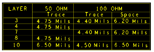
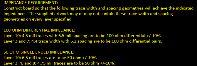
The impedance information must be included by the layout designer in the fabrication drawing notes. It should include impedance value, trace width, differential pair spacing, and the layer on which the controlled impedance traces are routed. An impedance table should also be included in the fab drawing. Below is an example of an impedance table.
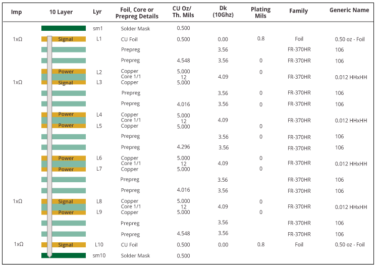
The figure below provides an example of how to specify controlled impedance in a fabrication drawing:
These notes will be reviewed by the PCB manufacturer, who will then build a stack-up to achieve the appropriate trace width and spacing as stated in the notes. To reach the required impedance value, they might make modest changes to these requirements.

Controlled Impedance Design Guide
6 Chapters - 56 Pages - 60 Minute ReadWhat's Inside:
- Understanding why controlled impedance is necessary
- Stack-up design guidelines
- How to design for impedance
- Common mistakes to avoid
Download Now
Statement of work (SOW) for CI documentation
A statement of work (SOW) is practically never requested for small manufacturing runs that offer rapid prototyping services. Designers or customers just need to submit the design data via an online portal or email, and the manufacturer will quote it and start production if it passes some simple DFM tests. Only for larger orders, the customer needs to provide a statement of work, to which the fab house will add a list of requirements. Customer approval is necessary before starting the production process.
When talking to a PCB manufacturer, it is a good practice to put together an SOW or a list of specifications with controlled impedance requirements. If a customer asks for a complete design review, the manufacturer will check the stack-up and routing to ensure the requirements mentioned in SOW are met.
Should you specify dielectric thickness or layers with target ohms?
There are two techniques to achieve controlled impedance:
- By only indicating the dielectric thicknesses in the fabrication drawing and not specifying any of the other controlled impedance parameters
- By indicating the layers on which impedance lines should appear, along with the target ohms
The standard tolerance is ±10% ohms. We offer ±5% ohms if a tighter tolerance is required. With new tools and precise data on PCB materials, manufacturers are able to model regulated impedance accurately.
Controlled dielectric thickness
The manufacturer receives the controlled dielectric stack-up from the designer. The production focus is only on constructing a board with a dielectric thickness tolerance of ±10% from layer to layer since the impedance traces are not defined.
Impedance control
The dielectric thickness, trace width, and spacing are used to control the impedance. Appropriate constraint setting on the design is essential to achieve controlled impedance. The manufacturer performs a test to check if the time-domain reflectometry (TDR) coupons can reach the necessary impedance. Certain modifications are made based on the findings of the first article inspection reports, and then the boards are manufactured within the specified tolerance.

PCB Material Design Guide
9 Chapters - 30 Pages - 40 Minute ReadWhat's Inside:
- Basic properties of the dielectric material to be considered
- Signal loss in PCB substrates
- Copper foil selection
- Key considerations for choosing PCB materials
Download Now
How to measure controlled impedances, if not specified?
A designer may think that by simply defining the specifications the impedance of the traces will be corrected. As previously stated, characterization is required for each manufacturing process to verify that it is matching the nominal values generated by field solver calculations. A manufacturer needs to work with the designer and help them realize why the field solver test is necessary.
Example of stack-ups demonstrating impedance requirements
Many factors influence the stack-up design parameters and choices (such as impedance, physical structure, blind holes, and so on). The impedance of signal lines is affected by the stack-up structure characteristics. Changing the stack-up parameters help attain target impedance. It is equally important to examine and balance other aspects in design that impact the stack-up. Consider the following:
- The thicker the dielectric thickness, the higher the impedance
- The smaller the dielectric constant, the greater the impedance
- The thicker the copper weight, the lower the impedance
- The impedance value will be higher if the dielectric constant is less
- A greater inductance indicates a higher impedance
- A higher capacitance indicates a lower impedance
At Sierra Circuits, we use tools such as Instack and Polar to design the stack-up. In these tools, the target impedance is entered along with the layer designation and other parameters such as Dk, dielectric thickness, type of material. These tools then generate a report, as shown below.
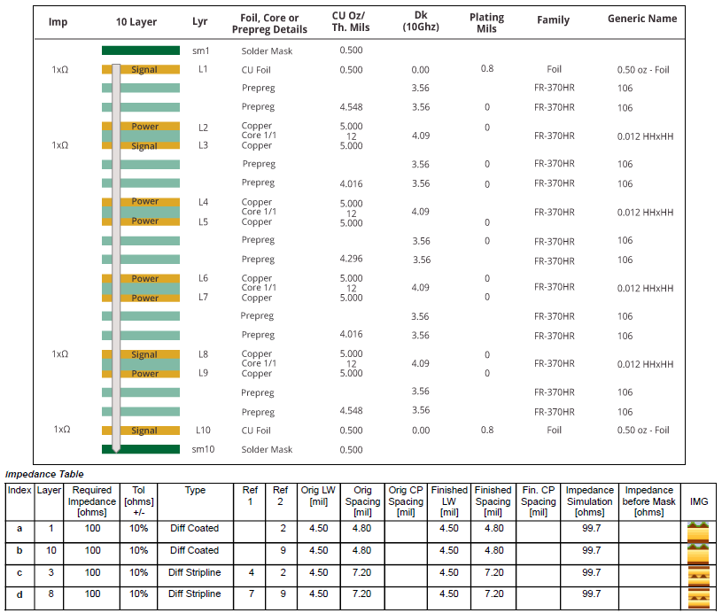
The report shown above has two parts: the first part shows the number of layers and details of the dielectric thicknesses and copper thicknesses. It also shows the thickness of the plating on the top and bottom layers. The material used in this case is FR-370HR. The second part shows the impedance table which gives the details of impedances on different layers along with the trace widths and trace spacing. For example, row ‘a’ above shows details of layer 1 (100 ohms) on a differential pair with a trace width of 4.5 mils and spacing of 4.8 mils. Similarly, information on other layers can be checked.
Why do manufacturers change the trace width and spacing?
Consider if the material is available in the desired thickness. The common core dielectric thicknesses are 3 mils, 4 mils, 5 mils, 6 mils, 8 mils, and so on. Prepreg glass styles 106, 1080, and others are common.
The material thickness is listed on the material data sheets or can be obtained from the laminate manufacturers. The quantity of resin in the prepreg, the amount of copper area %, and the thickness of the neighboring copper layers are used to compute the ultimate press-out thickness. From the CAD files, PCB manufacturers compute the percentage of copper area. As a result, they deviate from the datasheets’ general thickness specifications. They stick to their impedance modeling press-out thicknesses, which vary from design to design.
This will necessitate minor changes to the width and spacing of impedance traces. When the manufacturers are unable to fulfill the controlled impedance requirements they will recommend a different dielectric thickness or PCB material.

Impedance control verification
Test coupons are used to verify impedance control after the PCB has been manufactured. A test coupon is a board used to test the quality of the fabrication process. Test coupons are fabricated at the edges of the panel. Coupons are then inspected to ensure proper layer alignment, electrical connectivity, and internal structures. These are custom-designed for a circuit board or selected from a vendor library.
Test coupons are often placed at various positions on the working panel, representing a good cross-section of the PCB. The impedance is measured with a TDR. Following that, a report will be generated to indicate if the characteristic impedance is achieved or not.
When working on documentation for controlled impedance, it is critical for board designers to understand the best approach to express their requirements. Even if the requirement is minor, it still needs to be communicated clearly as a missing piece of data might make it difficult or impossible for the manufacturer to determine exactly what the customer requires.
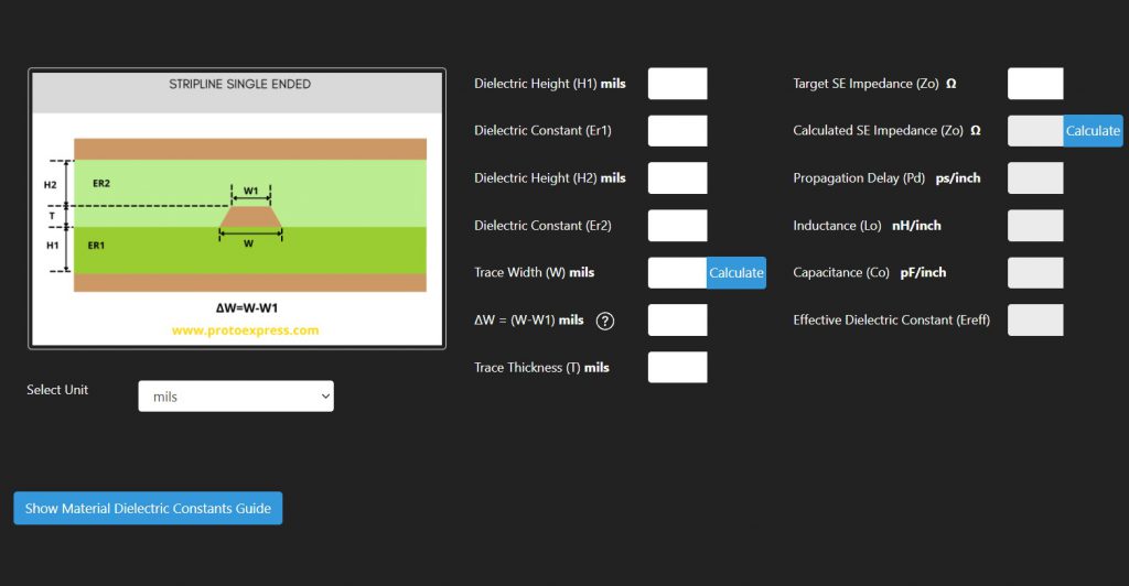
Try Sierra Circuits’ new Impedance Calculator
We have upgraded our Impedance Calculator, a free 3D field solder, which now uses the 2D numerical solution of Maxwell’s equations for PCB transmission lines. It renders accurate results suitable for use in circuit board manufacturing and engineering analysis. In addition to characteristic impedance of a transmission line, the tool also calculates line parameters such as capacitance, inductance, propagation delay per unit length, effective dielectric constant of the structure, and in the case of differential pairs, coupling coefficient, and even and odd mode characteristic parameters.
If you have any queries regarding controlled impedance, let us know in the comments section below.


