Contents
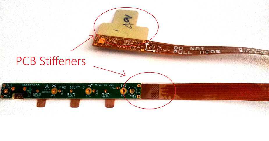
When designing a flex board, you need to consider whether certain areas require added rigidity for components or connectors, making PCB stiffeners an important part of the design process.
For instance, use FR4 when high mechanical support is required. Likewise, choose Kapton when added thickness with flexibility is required, especially for zero insertion force (ZIF) connector applications.
Highlights:
- Use stiffeners to reinforce areas containing SMT or through-hole components.
- Choose FR4 for rigid support during assembly and handling.
- Select polyimide supports when flexibility and added thickness are both required.
- Reduce stress at rigid-to-flex transition areas with proper stiffener placement.
In this article, you’ll learn what stiffeners are, why they are used in flex circuits, common materials and thicknesses, design considerations, and the differences between rigidized and rigid-flex boards.
What is a stiffener in a flex PCB?
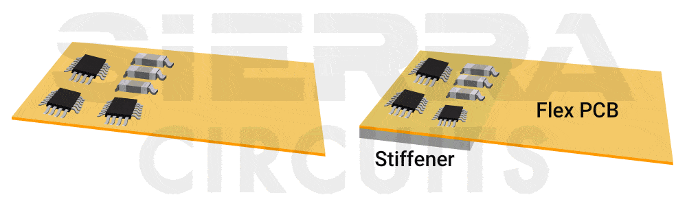
It is a rigid support material added to a flex printed board to reinforce certain areas. It is not a part of the electrical circuit, but it improves durability and provides mechanical support to the circuit board during assembly.
Flex boards offer many advantages, but they can lack stiffness in certain areas. To solve this, stiffeners are added to provide mechanical support where rigidity is required, such as near connectors, components, or mounting points.
What are the uses of stiffeners?
A stiffener is used to harden specific areas of a flex circuit that require added rigidity. It limits bending in those sections and helps protect the integrity of component solder joints.
Common uses include:
- Providing mechanical support for areas containing SMT or through-hole components.
- Adding thickness where required for connectors or assembly processes.
- Improving handling of thin, flexible circuit boards during manufacturing.
- Creating flat and stable surfaces for SMT pads or component placement.
- Preventing flex material stress caused by component weight in flexible zones.
- Reducing connector pad stress from repeated insertions, including zero insertion force (ZIF) connector applications.
- Increasing the bend radius at rigid-to-flex transition areas to reduce stress during repeated bending.
- Reinforcing sections used in panelization or array processing during manufacturing.
- Improving solder joint durability and resistance to mechanical wear.
- Assisting with heat dissipation in selected applications.
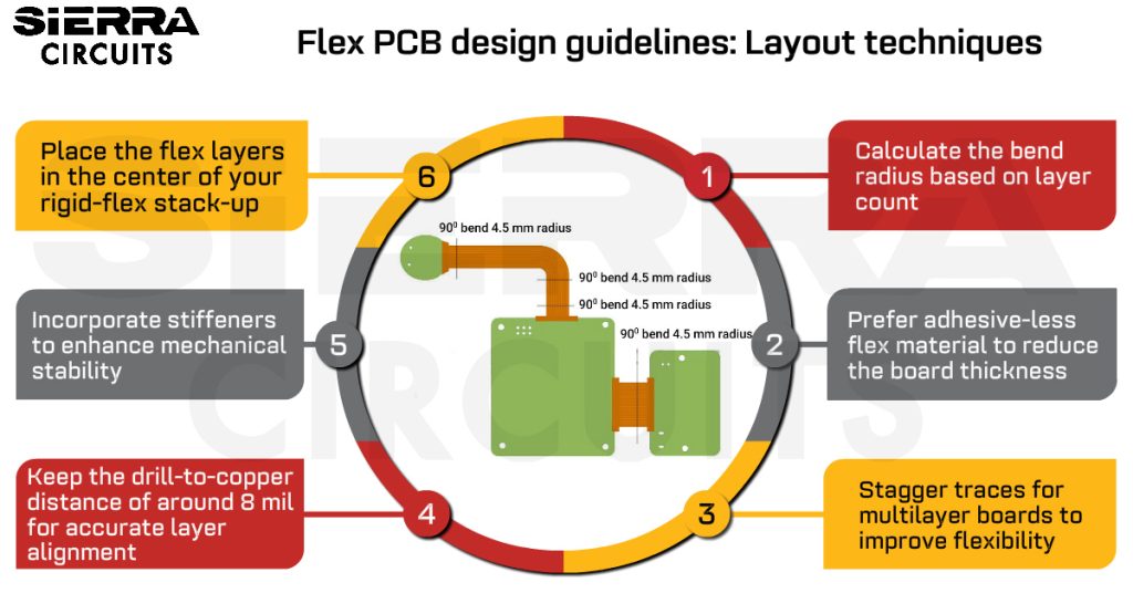
For more on flex layout, download our Flex PCB Design Guide.
Flex PCB Design Guide
10 Chapters - 39 Pages - 45 Minute ReadWhat's Inside:
- Calculating the bend radius
- Annular ring and via specifications
- Build your flex stack-up
- Controlled impedance for flex
- The fab and drawing requirements
Download Now
What materials are used for flex board stiffeners?
Typically, stiffeners are made up of FR4 or rigid polyimide (PI).
FR4 is a woven glass-fiber laminate impregnated with epoxy resin. Polyimide is produced using a high-temperature polymer formed into a thin film layer. Numerous layers can be stacked to attain greater thickness. Kapton is one of the classic polyimides used in PCB stiffeners. Kapton is frequently used when the flex ends need to be thickened and inserted into a ZIF connector.
In certain situations, you may need to use other materials, such as stainless steel or aluminum, for reinforcements. However, these materials are more expensive.

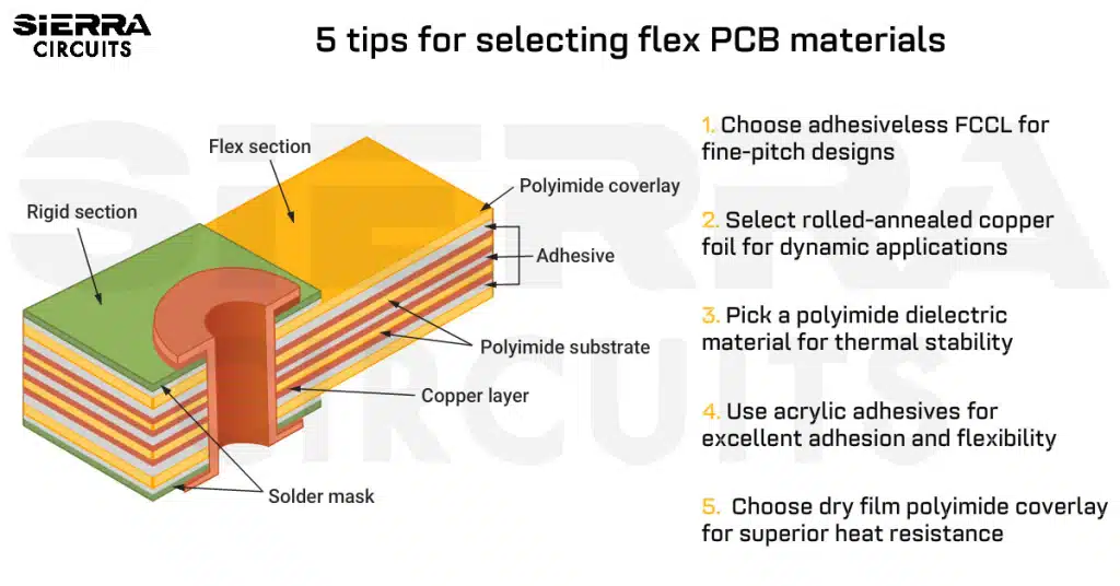
For more, see how to pick the right flex PCB materials for your application.
What are the typical thicknesses of stiffeners?
The thickness typically ranges from 0.002″ to 0.059″.
- Kapton is usually 0.002″ to 0.010″ thick.
- Rigid stiffeners such as FR4 typically range from 0.008″ to 0.059″.
The thicker the stiffener is, the more support it will offer. But every design seeks a different thickness. If you want your circuit board to be thicker, you will have to use polyimide supports.
Download the PCB Material Design Guide to learn how to pick the right laminates.

PCB Material Design Guide
9 Chapters - 30 Pages - 40 Minute ReadWhat's Inside:
- Basic properties of the dielectric material to be considered
- Signal loss in PCB substrates
- Copper foil selection
- Key considerations for choosing PCB materials
Download Now
How to use PCB stiffeners?
When using a stiffener for plated-through hole (PTH) components, the support material should be located on the same side of the flex circuit where the components are inserted. This allows access to the solder pads on the flex circuit. Stiffeners can also be attached to both sides of a part, but the printed board assembly may then require an array configuration review.
When an assembly array is required for flex circuit designs, it is common and cost-effective to include the FR4 reinforcement throughout the array border. This results in a rigid array and, in most cases, allows the parts to run through automated assembly in the same manner as a rigid circuit board design. It also eliminates the need for additional tooling plates.
Typically, we will use heat and pressure (thermal bonding) to attach the stiffener to the circuit. We can also attach it with a pressure-sensitive adhesive.
The two popular types of adhesives generically fall under pressure-sensitive adhesives (PSA) and thermally bonded adhesives. The selection of the adhesive depends on the various performance requirements, like thermal exposure, chemical resistance, and adhesion to various materials.
Sierra Circuits fabricates and assembles high-performance flex boards engineered to withstand harsh environments and support dynamic applications.
Check out flex PCB capabilities to learn more.
Difference between rigidized and rigid-flex boards
| Aspect | Rigidized PCB | Rigid-flex PCB |
|---|---|---|
| Structure | A flex board bonded with FR4 support to strengthen rigidity during assembly. | A hybrid flex circuit involving rigid and flexible substrates laminated into a single structure. |
| Primary function | Provides mechanical support to the flex. | Electrical connection between rigid and flex sections. |
| Traces on the rigid part | No traces on the rigid part, even on the pads. | Both the rigid and flex parts are designed with traces and connected by via holes. |
To know more about rigid-flex PCBs, read our article rigid-flex cuts electronic product assembly costs.
3 important stiffener design considerations
- Stiffeners should overlap the bared coverlay by 0.030″ (30 mil) to help relieve stress. It acts as the solder resist for the flex board.

Stiffener should overlap the bare covelay by 30 mil. - Maintain consistent stiffener thickness when using multiple supports in the same design.
- Align its thickness with the connector insertion and overall assembly requirements.
To know more about flex design considerations, check out Avoiding Common Flexible PCB Errors and Designing for Success
Sample rigid-flex stack-ups with stiffeners
Let us have a look at a few examples of rigid-flex stack-ups with stiffeners.
1. Two-layer flex stack-up with FR4 support

2. Two-layer flex stack-up with Kapton


3. Four-layer flex stack-up with Kapton reinforcements

At Sierra Circuits, we control curing parameters like temperature, pressure, and time to minimize stress and prevent layer misalignment in hybrid stack-ups.
To learn more, talk to a PCB expert: Book a meeting or call us at +1 (800) 763-7503.
We use a stiffener when we require a rigid area in our flex circuit to protect components or connectors attached there. This will prevent the circuit from bending, and the integrity of the solder joints is shielded. FR4 materials are commonly used for stiffeners; this material can be attached with thermally cured acrylic adhesive or pressure-sensitive adhesive. This serves our requirement of rigidizing the specific area in our flex circuit.
To learn more about rigid-flex design, read IPC-2223 standards and design violations for rigid-flex boards
Have queries regarding your flexible PCB designs? Post them on our community, SierraConnect. Our design experts will answer them.

About Milan Yogendrappa : Milan Y is an electronics and communication engineer with over 6 years of experience in developing and editing technical articles related to PCB design, manufacturing, and assembly. He is currently the editor-in-chief at Sierra Circuits.