


Contents

On-demand webinar
How Good is My Shield? An Introduction to Transfer Impedance and Shielding Effectiveness
by Karen Burnham
IPC class 2 and class 3 PCBs are built with stringent quality and reliability standards. Class 3 boards are the preferred choice for military and medical applications, whereas class 2 boards are ideal for dedicated electronic products like televisions, computers, and air conditioners.
Class 1 boards are tailored for general electronic devices with basic functions and a limited lifespan, such as the ones you can find in remote controls.
As a PCB manufacturer, we frequently receive inquiries from designers about the distinctions among IPC class 1, class 2, and class 3 boards. The selection of your board class depends on the specific application it serves.
Highlights:
- Class 3 allows no visual or functional defects, while class 2 permits limited cosmetic imperfections.
- Minimum barrel fill is 75% for both class 2 and class 3, with specific 50% fill exceptions allowed only for class 2.
- Class 3 requires stricter inspection, testing, and documentation.
- The IPC-2221 A/B test coupon examines the internal defects, and the IPC-2221 D coupon inspects the thermal stress on the class 3 boards.
What are IPC class 3 PCB design and manufacturing essentials?
IPC class 3 PCB design and manufacturing focus on the highest reliability requirements, with stricter tolerances, robust materials, and enhanced inspection controls for mission-critical electronics. The infographic below summarizes class 3 requirements.

Class 1: General electronic products
Class 1 boards are assigned to general electronic devices with a limited life and a simple function. This class includes the most typical everyday products. The class 1 boards allow various cosmetic defects as long as it doesn’t affect the functioning of the board.
The reliability of the product isn’t a critical factor in these types of boards. For instance, they can be found in LED lights, kids’ toys, etc. They are the most inexpensive boards to manufacture in the industry, but they come with a limited life expectancy.
Class 2: Dedicated service-electronic products
Class 2 boards are more reliable and have an extended life. They follow more stringent standards than class 1 boards but allow some cosmetic imperfections.
Uninterrupted service is preferable but not critical here. Class 2 products aren’t exposed to extreme environmental conditions. The board is expected to run continuously, but its operation is not extremely critical.
These kinds of boards are implemented in laptops, smartphones, tablets, communication equipment, etc.
Class 3: High-performance electronic products
John Perry, Director of Printed Board Standards and Technology at IPC, explains:
“Class 3 includes products where continued high performance or performance-on-demand is critical, product downtime cannot be tolerated, end-use environment may be uncommonly harsh, and the product must function when required.”
Class 3 boards must provide uninterrupted service even in harsh operating environments. There can be no equipment downtime. High levels of inspection and testing are performed on these boards with stringent standards.
This makes them highly reliable. Apart from complying with class 3 standards, these boards should also meet the additional requirements mentioned in the IPC 6012F document. It sets benchmarks for the boards used in military, medical, and automotive applications.
Key IPC addendums for class 3 applications
- IPC-6012FS addendum: This defines the standards for class 3 boards used in the space and military avionics industries. The standard describes PCB requirements to withstand vibration, ground testing, and thermal cycling.
Additionally, in acceptance testing, factors like acceptance criteria, sample size, and test frequency are changed.
Sierra Circuits manufactures extremely reliable mil-grade PCBs. Visit our aerospace and defense capabilities to learn more.
- IPC-6012EM addendum: The healthcare system utilizes surgical devices, X-rays, radiation, and ultrasound machines. Failure in these systems can directly put the patient’s life at risk. As a result, IPC has issued the IPC-6012EM addendum, which includes more stringent requirements for PCBs used in medical applications.
This is the only global industry-consensus standard that details qualification and performance specifications for rigid boards in medical applications.
The IPC D-33AM task group has created this document and mainly focuses on:
-
- Boards that are standard-sized and mass-produced.
- High-density interconnect boards are used in human body implants. It addresses miniature features like trace widths/spaces below 60 µm (2.3 mil) and via structures below 100 µm (4 mil).
- IPC-6012FA addendum: This provides additional documents, drawings, and specific requirements to the existing IPC-6012F for boards used in the automotive industry. It addresses the vibration and thermal cycling of the automotive environment. This addendum sets the specifications for:
-
- Lifted pads
- Dielectric removal (e.g., wicking)
- Accuracy in pattern features
- Solder mask thickness
- Cleanliness
- Reliability testing parameters
Read 10 automotive PCB design guidelines to learn class 3 design specifications for automobiles.
The major difference among all these classes is the degree of inspection. The IPC defines the permissible defects while manufacturing the boards.
The IPC also states that the bare board manufactured (before assembly and testing) should meet the specified class. That means a class 2 bare board cannot be deemed class 3 even after a perfect assembly and testing process.
Download our eBook to learn how to design class 3 boards.

IPC Class 3 Design Guide
8 Chapters - 23 Pages - 35 Minute ReadWhat's Inside:
- IPC guidelines for manufacturing defects
- IPC standards for assembly processes
- Common differences between the classes
- IPC documents to set the level of acceptance criteria
Download Now
General distinctions between IPC class 2 and class 3
The differences between IPC class 2 and class 3 PCBs are summarized in the infographic below.

| Specifications | Class 2 | Class 3 |
|---|---|---|
| Design rules | These boards are relatively simple compared to Class 3. Design rules for vias, plating, and tolerances are more relaxed as long as functional requirements are met. | Design rules are stringent, with layout, routing, and component placement carefully controlled to achieve maximum reliability and consistent performance. |
| Manufacturing constraints | Commonly used in high-volume consumer electronics. Minor defects are acceptable. It requires lower manufacturing time and budget. | Typically produced in lower volumes. Manufacturers follow strict specifications, increasing cost, turnaround time, and reliance on advanced fabrication equipment. |
| Inspection methods | Mainly visual, combined with basic functional testing to confirm acceptable electrical performance. | Extensive and includes microscopic analysis, advanced electrical testing, and environmental stress tests such as thermal cycling and vibration testing. |
What are the differences between class 2 and class 3 in assembly?
Umut Tosun, Application Technology Manager at Zestron America, explains:
“The major differences between IPC class 2 and class 3 are found in component placement for surface-mount components, cleanliness requirements based on residual contaminants on the assemblies, plating thicknesses as defined in plating through-hole and on the surface of PCBs.”
During assembly, the SMD might be slightly placed off the pad. This is what we call a visual defect since it does not usually affect electrical and mechanical performance. Therefore, it does not matter for class 2 circuit boards.
However, class 3 does not accept any imperfection, and this type of assembly misstep will cause the circuit board to fail the inspection.
| Assembly class | Part placement requirement |
|---|---|
| Class 2 | Can be slightly placed off the pad (considered a visual defect, it doesn’t affect the electrical and mechanical performance). |
| Class 3 | Imperfections are not acceptable, including visual flaws. This kind of imperfection will cause the circuit board to fail the inspection. |
The solder joints for class 3 boards should not have any voids, cracks, or defects. However, minor visual defects are allowed in class 2.

According to the IPC-A-610 revision H (the latest revision), the acceptable conditions for barrel fill are as follows:
- Acceptable condition for classes 2 and 3:
- Minimum 75% barrel fill.
- Up to 25% total depression (combined source and destination sides) is allowed.
- Exceptions for acceptable conditions for class 2:
- PTH component with 14 or more leads:
- Minimum vertical fill of 50% or 1.2 mm (0.05 in), whichever is less, provided all of the following are true:
- The component lead is visible on the source side of the solder connection.
- Surrounding PTHs meet solder requirements as per IPC-A-610H.
- Minimum vertical fill of 50% or 1.2 mm (0.05 in), whichever is less, provided all of the following are true:
- PTH component with 14 or more leads:
-
- PTH component with less than 14 leads:
- Minimum vertical fill of 50% or 1.2 mm (0.05 in), whichever is less, provided all of the following are true:
- The PTH barrel connects to internal thermal/conductor planes.
- The component lead is visible on the source side of the solder connection.
- Solder on the destination side has wetted 360° around the barrel wall and the component lead.
- Surrounding PTHs meet solder requirements as per IPC-A-610H.
- Minimum vertical fill of 50% or 1.2 mm (0.05 in), whichever is less, provided all of the following are true:
- PTH component with less than 14 leads:

| Assembly class | Requirement | Conditions |
|---|---|---|
| Class 2 | ≥75% fill, or ≥50% fill if exception applies | Exceptions:
|
| Class 3 | ≥75% fill (no exception) | All supported holes |
The circumferential wetting of lead and barrel on the solder destination side must be at least 180° for class 2 assemblies and 270° for class 3 assemblies.
As it can be delicate to get the paste into small plated through-holes (PTH), Sierra’s advice is to design your PTH 15 mil over the diameter of the lead. This way, you will have 7.5 mil on each side, which will make it easier for the paste to fill the barrel.
What are the differences between IPC class 2 and class 3 in PCB manufacturing?
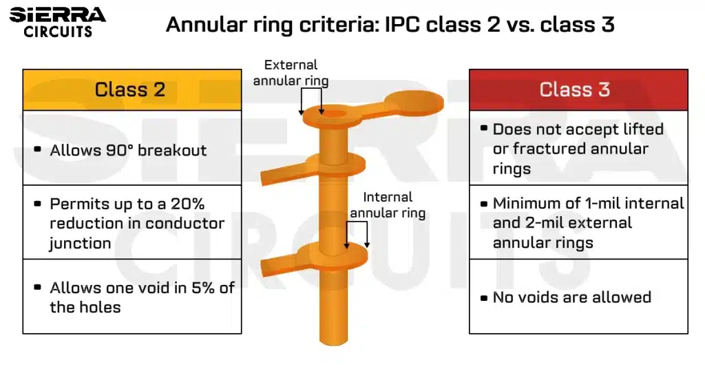
The key distinction between IPC class 2 and 3 lies in annular ring integrity. Class 2 permits controlled breakout, whereas class 3 requires near-perfect hole-to-pad registration with stricter minimum ring requirements.
Annular ring and drill breakout

Another factor in which IPC classes differ is drill breakouts. The distinctions are outlined below:
- For class 2, a 90-degree breakout of the hole from the land is allowed, provided minimum lateral spacing is maintained. Class 3 does not accept lifted or fractured annular rings.


- For class 2, the conductor junction cannot be reduced by more than 20% of the minimum conductor width specified on the engineering drawing. The conductor junction should never be less than 2 mil or the minimum line width, whichever is smaller.
- For class 3, the minimum internal annular ring cannot be less than 1 mil. The external annular ring cannot be less than 2 mil. It is measured from the inside of the PTH barrel to the edge of the land pad and may have a 20% reduction of the minimum annular ring in isolated areas due to defects, like pits, nicks, pinholes, or dents.


There will be a difference between the designed annular ring and the manufactured/actual annular ring. This is due to a shift in materials during the manufacturing process.
To meet the class 3 requirements, Sierra Circuits uses Pluritec machines to discover the shift in material, software to re-scale the drill locations, and vision drilling to accurately place the drills.
IPC annular ring acceptance criteria
| Feature | Class 1 | Class 2 | Class 3 |
|---|---|---|---|
| Plated-through hole | 180° annular ring breakout from the land is acceptable, provided the minimum lateral spacing is maintained.
The land/conductor junction should not be reduced by more than 30% of the minimum conductor width. |
90° annular ring breakout from the land is acceptable, provided the minimum lateral spacing is maintained.
The land/conductor junction should not be reduced by more than 20% of the minimum conductor width. The conductor junction should not be less than 0.05 mm or the minimum line width, whichever is smaller. |
The minimum annular ring should not be less than 0.05 mm.
The minimum external annular ring may have a 20% reduction of the minimum annular ring. |
What are the design rules for annular rings?
To achieve acceptance for IPC class 2 and class 3, follow the tables below, published by Altium Designer. The first one gives the annular ring requirements for mechanically drilled through holes, blind, and buried vias on ½ oz copper:
IPC class 2 drill and pad diameter for 1/2 oz copper
| Drill | Pad | Anti-pad | PCB thickness | Aspect ratio |
|---|---|---|---|---|
| 0.006” | 0.016” | 0.026” | Up to 0.039” | 6.5:1 |
| 0.008” | 0.018” | 0.028” | Up to 0.062” | 7.75:1 |
| 0.010” | 0.020” | 0.030” | Up to 0.100” | 10:1 |
| 0.012” | 0.022” | 0.032” | Up to 0.120” | 10:1 |
| 0.0135” | 0.024” | 0.034” | Up to 0.135” | 10:1 |
IPC class 3 drill and pad diameter for 1/2 oz copper
| Drill | Pad | Anti-pad | PCB thickness | Aspect ratio |
|---|---|---|---|---|
| 0.008” | 0.023” | 0.033” | Up to 0.062” | 7.75:1 |
| 0.010” | 0.025” | 0.035” | Up to 0.100” | 10:1 |
| 0.012” | 0.027” | 0.037” | Up to 0.120” | 10:1 |
| 0.0135” | 0.028” | 0.038” | Up to 0.135” | 10:1 |
IPC class 2 drill and pad diameter for various copper thicknesses
| Copper thickness | Pad diameter over drill (≤ 8 layers) |
Pad diameter over drill (> 8 Layers) |
|---|---|---|
| 1/4 oz copper | 0.010” | 0.010” |
| 3/8 oz copper | 0.010” | 0.010” |
| 1/2 oz copper | 0.010” | 0.010” |
| 1 oz copper | 0.012” | 0.012” |
| 2 oz copper | 0.014” | 0.014” |
| 3 oz copper | 0.016” | 0.016” |
| 4 oz copper | 0.018” | 0.018” |
IPC class 3 drill and pad diameter for various copper thicknesses
| Copper thickness | Pad diameter over drill (≤ 8 layers) |
Pad diameter over drill (> 8 layers) |
|---|---|---|
| 1/2 oz | 0.013” | 0.015” |
| 1 oz | 0.015” | 0.017” |
| 2 oz | 0.016” | 0.018” |
Calculating the pad size based on the minimum annular ring size
You need to consider the via type, layer count, line width, and manufacturing cost when deciding the via pad size. For instance, if you have a large trace width, opting for a larger pad size is essential, irrespective of the via size.
Another critical factor is the CNC drill wander. It occurs when the drill does not hit the center of the pad. This results in an insufficient annular ring or causes a breakout. So, selecting the right land size is crucial. Here is the formula to calculate the pad size using IPC-6012 and IPC-2221 standards.
Pad size = finished hole diameter + 2 (minimum annular ring size) + fabrication allowance
The fabrication allowance mainly depends on the drill wander. As per IPC-2221, class C is the highest classification, with an allowance limit of 8 mils. Additionally, the annular ring is measured differently for internal and external layers.
For internal layers, it is measured from the edge of the drilled hole. Consequently, the external layers are calculated from the edge of the wall plating. Hence, the values differ depending on the plating thickness.
For class 3 boards, the minimum annular ring sizes are as follows:
- Inner layers: not less than 1 mil
- External layers: not less than 2 mil
For instance, let’s calculate the pad size for a 12 mil diameter via in a class 3 board. Here, the finished hole size will be 10 mil (2 mil plating thickness).
Pad size (external layer) = 10 + 2 (2) + 8 = 22 mil
Pad size (inner layer) = 10 + 2 (1) + 8 = 20 mil
Similarly, for classes 1 and 2, the minimum annular ring size can be 0 for the inner layers. We need to consider via plating thickness (1 mil) for external layers.
This is one of the safest approaches for calculating the pad sizes that will adhere to IPC class specifications. It will also have fewer breakouts and be more reliable.
Annular rings in class 3 boards require mechanical strength to withstand thermal tension while operating in harsh environments. This calculation is for the minimum annular ring with respect to IPC. However, based on your design requirement, you can increase the annular ring size as much as possible.
For class 3 boards, tear-dropped via pads are also mandatory. Adding these allows for thinner traces without reducing the via size and reduces the risk of the hole separating from the conductor.

For calculating the optimum conductor width for your design, check out the trace width calculator

Features:
- Computations are based on the IPC-2152
- 3-in-1 calculator: temperature rise above ambient, trace width, and maximum trace current capacity
- Evaluates trace resistance, voltage drop, and power loss
What are the PCB through-hole plating requirements?
Class 3 boards do not allow voids in copper. On Circuitnet, Paul Reid, Program Coordinator at PWB Interconnect Solutions, said, “A copper void is where the copper plating in the barrel of the hole is missing, exposing the dielectric material of the drilled hole.
Class 2 allows one void in 5% of the hole,s and class 3 allows no voids.” The plating thickness requirement for class 2 is 0.8 mil as opposed to 1 mil for class 3.
These are just a few requirements that differ between class 2 and class 3. As usual, the best advice we can give you is to communicate with your PCB manufacturer.
They will guide you and help you get it right the first time. You should also request a cross-section of your board to make sure that your shop meets your specifications. For a more detailed explanation, read our post on 6 DFM issues.
The IPC document also defines the following minimum requirements for surface and hole plating:
- Buried vias > 2 layers, through holes, and blind vias
- Microvia: blind and buried
- Buried cores: 2 layers
Refer to tables 3-4, 3-5, and 3-6 of the IPC 6012E version, March 2020.
Plating is usually measured as an average per side of the hole. Glass fiber protrusions into the hole’s plating can cause cracks. When calculating the average plating of the hole, such isolated thick or thin plating is ignored.
What’s new in IPC 6012 revision F?
Here are the latest updates seen in the IPC 6012 class 3 standards in September 2023:
1. Minimum dielectric thickness for IPC class 2 and class 3: 2.56 mil

The minimum dielectric thickness requirement for IPC class 3 and class 2 has been lowered to 2.56 mil. The organization made this change to facilitate the laser drilling process.
Most fabricators incorporate a dielectric thickness of 3 mil to 4 mil to achieve the required aspect ratio for the microvias. This results in non-compliance with IPC class 3 standards. The IPC 6012F update gives fab houses a leeway while building HDI boards.
PCB manufacturers will consider 2.56 mil as the default dielectric thickness for any fab drawing of class 3 boards submitted after 1/1/2024.
It is important to note that the thickness referred to is the press-out thickness after the lamination process.
2. PCB cavities: Type 1, type 2, and type 3
IPC 6012 revision F introduces new rules for cavities milled on a printed board. It classifies the cavities into three types and sets rules accordingly.
- Type 1: No metallization of floor or walls
- Type 2: Metallization of floor or walls
- Type 3: Metallization of floor and adjoining walls with continuous plating
Design considerations for PCB cavities include:
- Adhere to +/-0.005” of depth tolerance from the outer layer.
- Keep the conductors at least 0.020” away from the cavity edge to increase manufacturing yield.
- Place the plated holes 0.030” away from the cavity edge.
- Plate and fill vias in the cavity as per IPC-4761 Type VII.
- Avoid solder masks in cavities.
3. Default surface finish: ENIG
In the previous version, the default surface finish was tin/lead. However, most manufacturers prefer ENIG as it can be processed in-house, whereas tin/lead finishes are generally outsourced.
HASL (lead-free) finish was out-ruled as it consumes more electrical power, which increases the overall cost. Hence, if a document does not specify a surface finish, then the manufacturer considers ENIG as the default PCB surface finish.
4. Edge plating: Voids should be <0.050″
Here are manufacturing considerations for edge plating as per IPC 6012 rev F:
- Plating separation from the edge wall is not allowed.
- Plating voids should be within 0.050’’ and not more than 3 locations.
- Burrs and exposed copper are allowed on breakaway tabs.
- To promote copper adhesion, it is recommended that the top and bottom surfaces of the edge plating have wrap plating.
5. Plated internal layer: Refer to table 3-17 of IPC 6012 rev F
In the previous version (IPC 6012 E), it was not clear whether to use the table “Thickness of External Conductor of the Finished Printed Board after Plating” or “Internal Layer Copper Thickness after Processing” for the internal plated layer.
This confusion led to many rejections as the external conductor rule was used. If this rule were implemented, the conductor would be much thinner than the requirement.
Hence, in Revision F, it is confirmed that the internal plated layer will follow the lower total copper requirement as per table 3-17 of IPC 6012 rev F, Internal Layer Copper Thickness after Processing.
6. Dimples and protrusions: standards for dimples and bumps
Previously, dimples and protrusions were agreed upon between the customer and suppliers (AABUS). This is modified in Revision F. For microvias on land, you should follow the rules below:
| Hole diameter | Maximum dimple | Maximum bump/protrusion |
|---|---|---|
| Greater than 0.15 mm (0.0006 in) | 50 μm | 25 μm |
| Less than or equal to 0.15 mm (0.0006 in) | 25 μm | 25 μm |
7. Back drill depth: new guidelines for back drilling
In revision F, a new section (1.4.3) specifies the surface for measuring the depth of the back drill. Previously, it was evaluated using the copper foil or the total copper thickness.
Here are other guidelines for a back drill:
- Identify the side-to-back drill and the must-not-cut (MNC) layer.
- Review the design distance between the back drill diameter and conductors adjacent to the back drill path.
- Create a separate drill program for each back drill type and span.
- Develop a drill chart that specifies the back drill diameter with the count.
- Specify if the back-drilled hole should be epoxy-filled.
- Define the stub length allowance.
- Clearly state if the back drill should be plated over and attached to an external ground plane.
- Include instructions if the PCB fabricator must modify the data to achieve a finished copper ground fill over the back drill.
For more on back drilling, see what is back drilling in PCB design and manufacturing.
Why are PCB cross-sections critical for class 3 boards?
Cross-sections are critical for class 3 boards as they provide direct, microscopic proof of internal reliability that visual and X-ray inspections may not detect. To make sure that your PCB manufacturer meets your requirements, ask for a cross-section analysis.
This destructive technique, mostly using a microscope, is the best way to verify your board’s internal structure. The test can check for various aspects, such as cracks, voids in solder joints, through-hole filling, etc.
General procedure for conducting a cross-sectional analysis:
- Select a PCB sample from a production run.
- Isolate critical areas and cut perpendicular to the plane to expose the cross-section.
- Mount it onto a cross-section holder using a suitable adhesive.
- Polish the sample with abrasive papers.
- Using a microscope, examine the cross-section for defects.
- Compare the analysis to the requirements set forth in IPC class 3.
- Take digital photographs to record the identified defects (magnified to 100X).
Below is a cross-section of a class 2 circuit board:

This is a cross-section of a class 3 board:

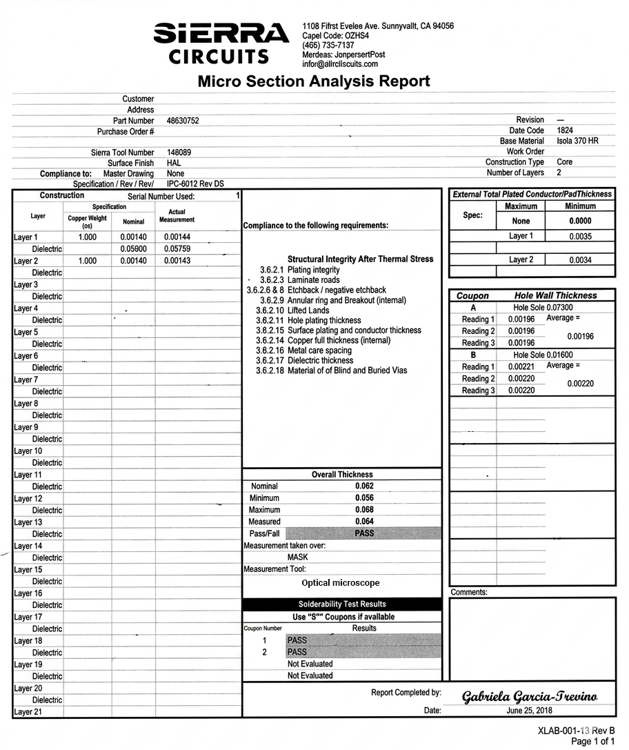
At Sierra Circuits, we do in-process cross-sections for every circuit board we manufacture at each step of the building process. We check for dielectric, plasma etch, solder mask thickness, copper, plating, etc.
And if we don’t meet the customer’s requirements, we reject the board and build another one. If you need a report, you can ask for a final cross-section. We will send a document with everything we tested and the results. The microsection analysis report looks like this:
3 test coupons to examine the internal defects of class 3 boards
IPC-2221 A/B, IPC-2221 D, and D coupons are used to detect internal defects and validate plating quality in class 3 boards.
You need to precisely communicate your test coupon requirements to your CM for a seamless testing procedure. Here’s what you need to include in your fab notes:
- Purpose of the test coupons.
- Drawing instructions (dimensions, shape, and layout of the test coupons).
- Pad sizes, trace widths, and line spacing on the coupons.
- Number of test coupons and the intended locations on the PCB panel.
Let’s have a look at the types of coupons used in class 3 PCBs:
1. IPC-2221 A/B coupon

The A/B coupon inspects both vias and component holes. The outer row is designated as test coupon A, and the inner row represents coupon B.
Test coupon A allows rework simulation of component holes and features large holes with a diameter of 1.905 mm. Whereas, coupon B evaluates the thermal stress of plated-through holes.
This coupon contains smaller holes with a diameter of 0.15 mm. Small PTHs are susceptible to increased tensile stress in the barrels near the central z-axis of the board.
2. IPC-2221 D coupon

IPC D coupons can effectively identify defects such as premature failure, plating voids, thin copper, interplane separation, cracked barrels, blind via to pad separation, and lifted lands.
These coupons are strategically positioned in all four corners and the center of the panel for each via structure to assess the interconnection resistance, continuity, and stack-up of your circuit board.
The coupon is equipped with a sufficient number of plated holes or vias connected in a daisy-chain fashion for the highest precision in resistance measurements.
3. IST testing with D coupons
IST imposes thermal stress on a coupon by cycling electrical current through a daisy chain of vias. If the coupon can withstand a minimum of 300-500 cycles before any change in resistance, it ensures the plating integrity of the circuit.
Testing procedure:
- First, the D coupons are subjected to 6 reflow simulations and 100 thermal shocks, as per IPC-TM-650.
- Resistance values are then monitored every second during reflow simulation and once per cycle during thermal shocks. If resistance changes by 10%, Via is reported as failed.
- The Propagated D coupon applies to structures with filled vias, blind vias, and buried vias. This coupon may contain up to two via structures, representing multiple drilling and plating steps.
(References: IPC-2221A and IPCB-2221B)
Inspection and acceptance criteria
After the product’s end-use, the degree of inspection should be taken into account when choosing which category your PCB should fall into. Keep in mind that inspection is one of the factors that drives up the cost when an assembly goes from class 2 to class 3.
When you think about it, PCBA is not a simple task. The board needs to properly function once assembled with all its components, materials, and solder to hold them together.
Depending on which class your board falls into, the requirements you will have to meet for inspection will differ. This is when some IPC documents come in handy to set the level of acceptance criteria for each product.
General inspection methods for checking IPC class 2 and class 3 boards include visual, AOI, X-ray, solderability, and electrical testing. However, the specs will be more stringent for class 3 PCBs.
Additional testing, such as micro-section analysis, and environmental tests, such as stress, pressure, vibration, and burn-in tests, are also conducted.
PCB design and manufacturing standards
On Circuitnet, Leo Lambert, Vice President of EPTAC, made a list of the most significant documents: the IPC 2220 series for circuit board design and fabrication, the IPC 6010 series documents for board performance and quality, IPC-A 600 for board acceptance requirements, J-STD-001 for soldering requirements, and IPC-A-610 for acceptability requirements.
There is a misconception that links class 3 boards only to the aerospace field. It is often true, but these circuit boards are not exclusive to aerospace or any other industry.
The criteria are based on the application of the product. Therefore, class 3 can also be the criterion for avionics, military, industrial, and medical applications.
It makes sense that many class 3 boards are for aerospace. Products launched into space have to be highly reliable to prevent critical failures. The additional inspection is just too pricey for the commercial and consumer market.
When you require a class 3 circuit board, it implies that the product has to be built according to the complete IPC criteria.
This means the design and manufacturing teams must consider the following factors:
- Laminate selection
- Plating thickness
- Annular ring requirements
- Manufacturing processes
- Facility arrangements
- Inspection criteria
To learn how to design a manufacturable board without board respins, download our handbook.

Design for Manufacturing Handbook
11 Chapters - 96 Pages - 90 Minute ReadWhat's Inside:
- Annular rings: avoid drill breakouts
- Vias: optimize your design
- Trace width and space: follow the best practices
- Solder mask and silkscreen: get the must-knows
Download Now
As a designer, it is essential to know the IPC design and manufacturing standards that best suit your design. By following the benchmarks, you can build a high-quality board while eliminating board re-spins and lowering overall costs.
Let us know in the comments section if you have any questions related to IPC classes; our design and manufacturing experts will be happy to help you.


This post on class 3 design rules specifies a 3.54 mils minimum dielectric thickness (now 2.56 with 6012F), but IPC-6012 specifies this requirement applies only if the minimum dielectric spacing is not specified in the procurement documentation. So if I specify Class 3 on the fab drawing with a minimum dielectric spacing of X (say 2.3 mils) and Sierra agrees to manufacture it, I’m golden? Breakdown voltage on test coupons covers it? What IPC standard specifies what test coupons and tests must be applied to a Class 3 board?
Some of this has changed so will have better answer on Monday. The short answer for now is if a customer sends us a Class 3 job, we would review and make sure it meets all the requirements. We wouldn’t accept your data and call it good. Our CAM scripting automatically generates all the test coupons when Class 3 is specified.
“make sure it meets all the requirements”: that’s my point, what is the requirement for dielectric thickness? Fab shops are typically quoting the 3.54 mils (now 2.56 with 6012F), but the standard only requires that if the minimum dielectric spacing is not specified in the procurement documentation. Sounds like a loophole in the standard.
Finally got a good answer on this. The standard was 3.54 mils. It can now go down to 2.56 mils as long as the specification drawing is dated after 1/1/2024. These are default minimums that must be met. If the procurement documentation calls for something less it will not meet Class 3 and would need to be questioned. There isn’t a loophole.