


Contents
A PCB fab drawing should include the board outline, drill chart, layer stack-up, fabrication notes, tolerances, and material specifications required to manufacture the bare board.
In this article, you will learn what information a PCB fab drawing should contain, why each section matters for manufacturing, and how to generate fabrication drawings in KiCad, Eagle, and Altium Designer.
Highlights:
- A fabrication drawing defines the mechanical, material, drilling, and stack-up requirements.
- Fab and assembly drawings serve different purposes: one defines bare board construction, while the other defines component placement requirements.
- Clear fabrication notes help prevent manufacturing assumptions related to surface finish, via structures, solder mask, plating, and tolerances.
What is a fab drawing?
It is a technical blueprint that communicates board geometry, layer architecture, and manufacturing specifications to a fabricator. Unlike standard layout files, this document provides explicit dimensional data, material requirements, and tolerances. Manufacturers rely on it alongside Gerber files to prevent misinterpretations during production.
Fab and assembly drawings are the key reference documents for manufacturing and inspection. The fab drawing defines board construction, while the assembly drawing defines component placement.
How is a PCB fab drawing different from an assembly drawing?
The fabrication document defines board construction requirements, while the assembly drawing shows component placement and assembly instructions.
| Feature | Fab drawing | Assembly drawing |
|---|---|---|
| Primary goal | Defines the physical bareboard construction (substrate, copper, apertures). | Outlines component placement and mounting requirements on the bare board. |
| Stakeholders | Designers and fabrication house | Designers and assembly facility |
| Key elements | Board outline, hole locations/sizes, and stack-up. | Component outlines (silkscreen), reference designators (R1, C1, U1), polarity marks (+/-, pin 1 dot). |
| Critical dimensions | Finished hole sizes, annular rings, and board edge tolerances. | Component clearances, height restrictions, and connector orientations. |
| Technical specs | Dielectric materials, copper weights, surface finish, and impedance targets. | Bill of materials (BOM) cross-references and soldering standards (IPC-J-STD-001) |
| Drill data | Comprehensive drill chart with tolerances and hole plating status. | Limited to mounting holes or mechanical hardware locations. |
| Data files | Gerber (X2), NC Drill files, and IPC-D-356 netlist. | Pick-and-place (centroid) files, BOM, and assembly-level PDFs. |
Download the PCB Fab and Assembly Notes for Designers.

PCB Fab and Assembly Notes for Designers
8 Chapters - 72 Pages - 70 Minute ReadWhat's Inside:
- Guidance on how to write comprehensive fab documentation
- Advanced fabrication notes for flex, rigid-flex, and hybrid stack-ups
- Difference between fabrication and assembly notes
- Assembly documentation essentials: BOM, X-Y data, and drawings
Download Now
What should you include in a PCB fabrication drawing?

A fabrication drawing should consist of the board outline, drill chart, layer stack-up, fabrication notes, tolerances, and material specifications. Let’s look at these in detail.
Board outline to determine the size and form factor
It defines the PCB shape, dimensions, cutouts, and mounting constraints required for fabrication and enclosure compatibility. Any fabrication drawing is incomplete without a pictorial representation of the circuit board. This includes all the cutouts, holes, different radii, and specific distances in the actual board.
All the dimensions are measured from an origin (0,0) point. This origin point on the fab drawing must be the same as that of the (0,0) point on the NC drill data file. The drilled holes are also pointed out in this drawing with symbols linking them to the drill chart.
Drill chart to represent plated and non-plated holes

A drill chart demonstrates all the particular symbols assigned to the drilled holes in the board outline. This chart contains information related to the drilled hole requirements of the circuit board to be manufactured. Drill symbols may be shapes or textual characters representing a hole’s position. These symbols are generated by the PCB layout software.
A drill chart features specific symbols with respect to the hole size. This chart also shows the number of holes of a particular size, whether plated or not, their hole tolerances, and so on.
Title block for a clear understanding
In the fab drawing, the title block identifies the PCB revision, customer name, part number, units, and fabrication references required for manufacturing traceability. It is not an absolute requirement for a fabrication drawing, but it is very helpful to have one.
Circuit board layer stack-up

The layer stack-up section of the fabrication drawing will convey information such as layer order, dielectric spacing, copper weight, material type, and the total thickness of the stack-up. The controlled impedance requirements are also indicated in the layer stack-up. The stack-up data allows the fabricator to adjust trace geometry and dielectric spacing to achieve the target impedance.

What additional notes should a PCB fab drawing include?
Apart from the above must-have information, your fab drawing should specify fabrication notes that define manufacturing requirements that are not fully captured in Gerber, drill, or stack-up data. Let’s look at the notes below:
- Controlled impedance requirements: To achieve the desired controlled impedance, trace thickness, trace width, trace distance from the reference planes, and dielectric constant should be varied accordingly. Any basic impedance calculator can be used for this.
- Board manufacturing specifications.
- Designation of the board’s primary side.
- Raw material specification for the boards: These should meet all the required standards.
- Plating details.
- Solder mask and associated specifications (color, finish, etc.)
- Surface finish: If the surface finish is not specified, the fabricator may apply a default finish based on internal manufacturing standards.
- Gold fingers: If part of the circuit board construction, mention them in the fab drawing.
- All the critical mechanical specifications related to the hole position.
- Presence of via-in-pad/plugged via.
- Implementation of blind/buried via.
- Tolerances:
- Board tolerance (typically ±10%).
- Etching and plating tolerance.
Need help in preparing accurate fabrication drawings for your circuit boards? Check out our PCB design support.

How to create a fab drawing in Eagle EDA?
A fab document in Eagle EDA is prepared by generating Gerber and drill files and compiling the board outline, layer information, and fabrication details required for manufacturing. Eagle’s CAM Processor and drill configuration tools simplify the generation of fabrication outputs.
Generation of fab drawings in Eagle is simple and requires only a few steps. Once the design of the schematic is complete and the layout of the circuit board is ready with all the signals, then:
Step-1: Go to CAM Processor > GerberAuto. This will generate the Gerber file.
Step-2: Open Layout editor > Options/Set/Drill. This will allow you to use various drill symbols on the board. Once done, save the file in Excellon format and use this drill file in the fabrication drawing.
Step-3: Thus, all the information about the board material and the number of layers can be compiled.
Send all the above files to the manufacturer as fabrication drawings.
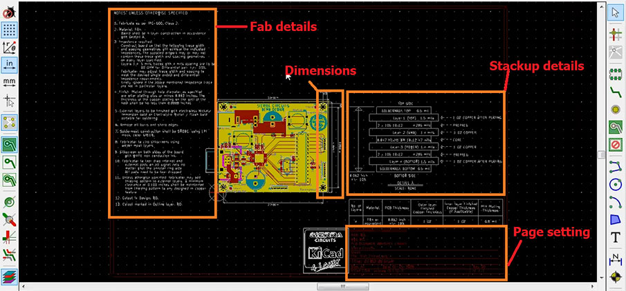
How to generate a fab drawing in KiCad?
Start by defining the title block, board dimensions, stack-up details, drill information, and fabrication notes on the fab layer. These details help manufacturers interpret the PCB requirements accurately during production.
In KiCad, first, you need to add the title block.
Step-1: Go to Files > Page settings. In the window that opens up, add all the details, such as title, company name, part numbers, etc., that need to appear in the title block.

Step-2: To include the text and logo of the company in the drawing, select the Silkscreen layer > Text icon > and click on the board at the desired location. A window will pop up to add and customize the text.

Step-3:For placing the logo, select Files > Import > Import Graphics.
Make sure you have the DXF file of the logo. Next, choose the DXF file and set the required dimensions.

Step-4: Add all the board dimensions to the outline. Click on the Add dimension icon > Fab layer.
Now, if you have to add the dimensions between two mounting holes, go to the center of the mounting hole. A circle will appear when the cursor is at the center. Click on that and then go to the next mounting hole and pull the dimension down. This will generate a line showing the distance between the two holes.

Once you input the dimensions, the graphics tool draws the stack-up in the fab layer. All the information, such as the layer thickness, solder mask thickness (top and bottom layer), board thickness, tolerances, etc., can be mentioned.
The text tool is used to mark the details mentioned above.
On the fabrication layer, you can add all the fab details. These include the IPC class of the board, the number of layers, the solder mask color, and so on. You can even mention the type of pads (plated or non-plated through-hole pads) and their tolerances.
Download our KiCad 9 Step-by-Step Guide to quickly understand the PCB design workflow.

KiCad 9 Step-by-Step Guide
6 Chapters - 41 Pages - 30 Minute ReadWhat's Inside:
- A complete KiCad 9 workflow from project creation to production file generation
- Step-by-step guidance on creating custom libraries and linking symbols to footprints
- Practical design checks: ERC and DRC
- Best practices for generating a clean BOM and fabrication-ready Gerber files
Download Now
How to create and save a PCB fab drawing in Altium Designer?
In Altium Designer, fabrication documents are produced by combining board layout data with drill tables, fab notes, and stack-up information in a dedicated drawing document. The tool automatically links fabrication data to the PCB database, ensuring updates remain synchronized with design revisions.
Step-1: Use a blank drawing format of the board and then add all the additional information, and add fab notes and drill charts.
Step-2: Compose or import the fab notes from a certain existing file.
You can easily obtain the drill files by following the steps below:
- Go to Place > Drill table. The drill table will be attached to the cursor, select a location outside the board layout, and press Enter to place it.
- To change the properties of the table before placement, press the Tab key and select the Drill table mode in the properties panel.
The tool automatically links all the files added in the fabrication drawing to its design database. This helps in the automatic update of the drawing corresponding to the changes in the design.
At Sierra Circuits, we fabricate and assemble circuit boards with controlled impedance structures, advanced stack-ups, and detailed fabrication documentation to meet complex manufacturing requirements.
To learn more, see our rigid manufacturing capabilities.
Fabrication drawings provide additional information that a Gerber file cannot convey to the manufacturer. There is no single universal format for fab drawings, so the document should clearly state all fabrication requirements to avoid assumptions.
A complete PCB fab drawing eliminates ambiguity and reduces manufacturing errors. Always include the board outline with dimensions, drill chart, detailed stack-up, and comprehensive fabrication notes. Providing clear, accurate documentation helps fabricators deliver boards that meet your specifications on the first run. For complex designs, review your fab drawing with your manufacturer before final production.
Have questions about creating fab drawings for your circuit boards? Post your queries on SierraConnect. Our PCB experts will answer them.


