Contents

On-demand webinar
How Good is My Shield? An Introduction to Transfer Impedance and Shielding Effectiveness
by Karen Burnham
Laser drilling creates precise holes on a PCB to establish connections between different layers. The sleek gadgets that we all are acquainted with consist of HDI boards that incorporate laser drills. This technique ensures accuracy even when dealing with the smallest of sizes.
As we know, laser stands for light amplification by stimulated emission of radiation. Laser drilling is the process that uses highly concentrated laser energy for drilling (vaporizing) a hole. It is completely different from drilling holes mechanically using a drill bit.
What is circuit board drilling?
Circuit board drilling is the process of drilling holes on the PCB for any of the purposes mentioned below:
- Placement of components
- To bring interconnection between different layers
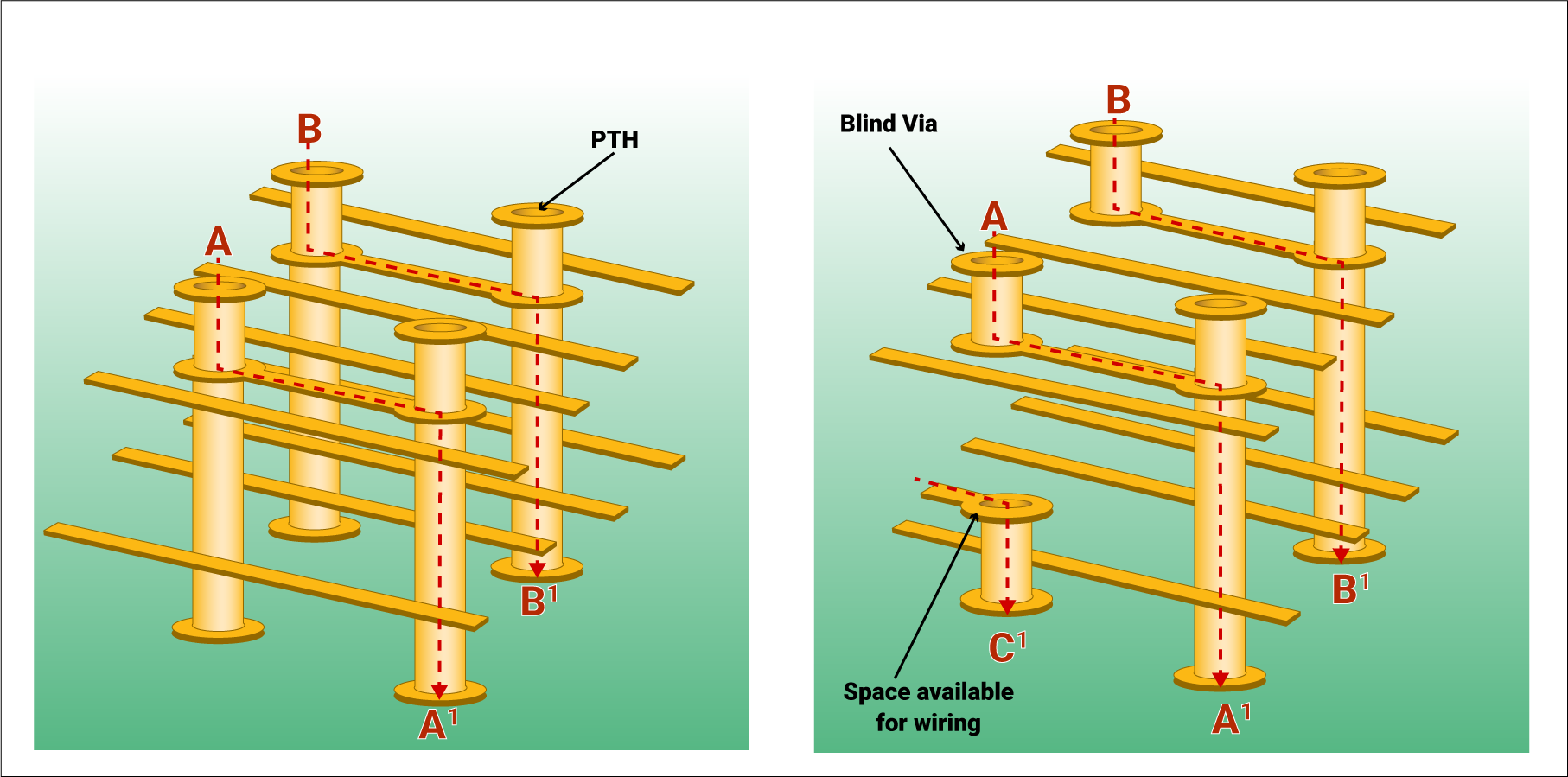
These are achieved by various types of vias namely through-hole vias, microvias, blind vias, and buried vias. When it comes to vias for electrical interconnection between layers, blind vias are preferred over through-hole vias. Blind vias increase the space available for wiring compared to the through-hole vias. It is demonstrated in the figure below.
Why is laser drilling required for circuit boards?
When using HDI technology for PCB designing, plenty of microvias are included. These microvias that appear to be blind structures are small in size and require precise controlled depth drilling. This precision can only be achieved using lasers.
Why mechanical drilling cannot be used for microvias?
Mechanical drilling is not suitable for microvias due to the following reasons:
- It incorporates a lot of moving parts and can’t achieve the positional accuracy of a laser
- Drill geometry in mechanical drilling doesn’t allow the formation of a flat capture pad
- Drilling in the 4-6 mil diameter range is very slow and expensive. Drill deflection/breakage, accuracy and hole quality are also issues in this size range
- Doesn’t have the required depth control

Design for Manufacturing Handbook
11 Chapters - 96 Pages - 90 Minute ReadWhat's Inside:
- Annular rings: avoid drill breakouts
- Vias: optimize your design
- Trace width and space: follow the best practices
- Solder mask and silkscreen: get the must-knows
Download Now
How small of a hole can a laser drill?
Lasers can drill 2.5 to 3-mil vias on a thin flat glass reinforcement. In the case of an unreinforced dielectric (with no glass), it is possible to drill 1-mil vias using lasers. Hence, laser drilling is recommended for drilling microvias.
What are the advantages of laser drilling?
The advantages of using lasers are listed below:
- Non-contact process: Laser drilling is a non-contact process, and hence the damage induced on the material by drilling vibration is eliminated.
- Precise control: We can control the beam intensity, heat output, and duration of the laser beam. This helps to create different hole shapes and offers high accuracy.
- High aspect ratio: One of the most important parameters of a drilled hole on a circuit board is the aspect ratio. It is the ratio between the drilled depth and the diameter of the hole. Since lasers can create holes with very small diameters, they provide a high aspect ratio. A typical microvia has an aspect ratio of 0.75:1.
- Multi-tasking: Laser machines used for drilling can also be used for other manufacturing processes like scoring, skiving, and milling.
How do you make micro-holes using lasers?
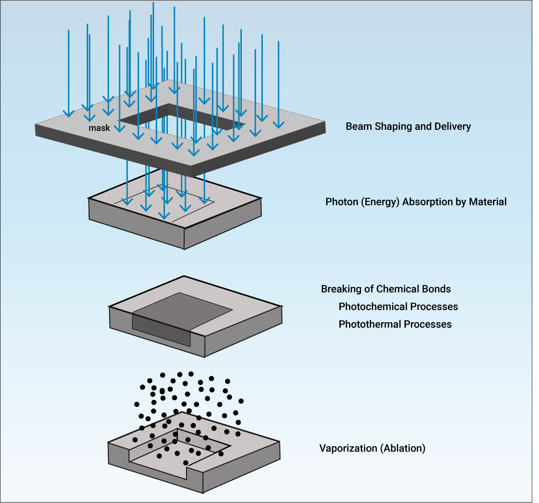
As we can see from the above figure, the laser beams are projected onto the material using beam shaping techniques. The material absorbs the beam energy which breaks the chemical bonds. This process of removing material from a surface by irradiating it with a laser beam is called laser ablation. These vapors will create a recoil pressure that exerts a downward force on the remaining molten material.
The recoil pressure will force the molten material to flow out of the hole. The ejection of the molten material is termed melt ejection. The absorption rate depends upon the type of material used. Usually, we use non-homogeneous materials like FR4 for circuit boards.

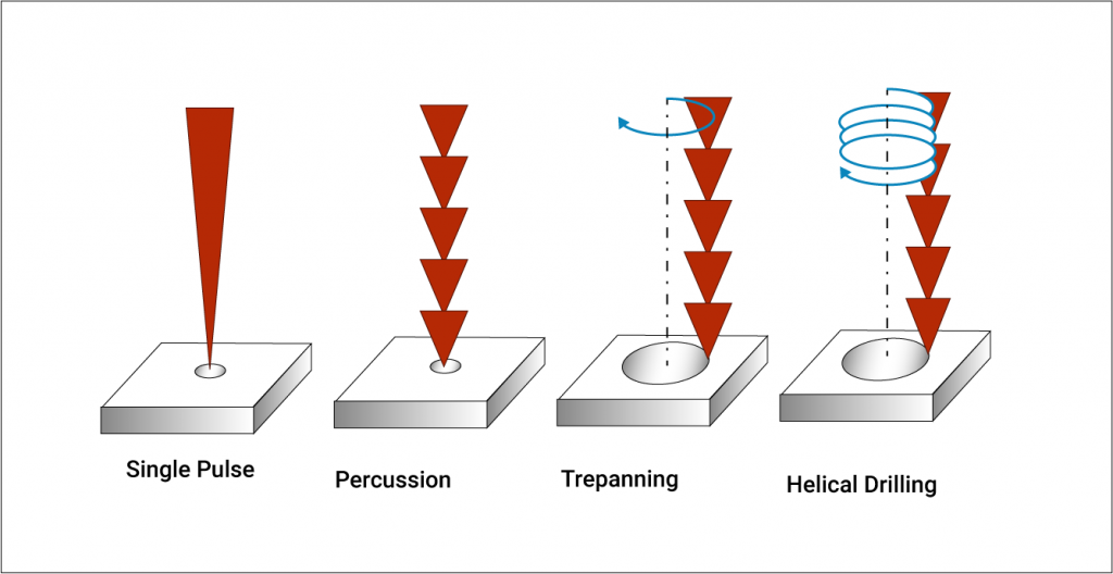
Different methods of laser drilling
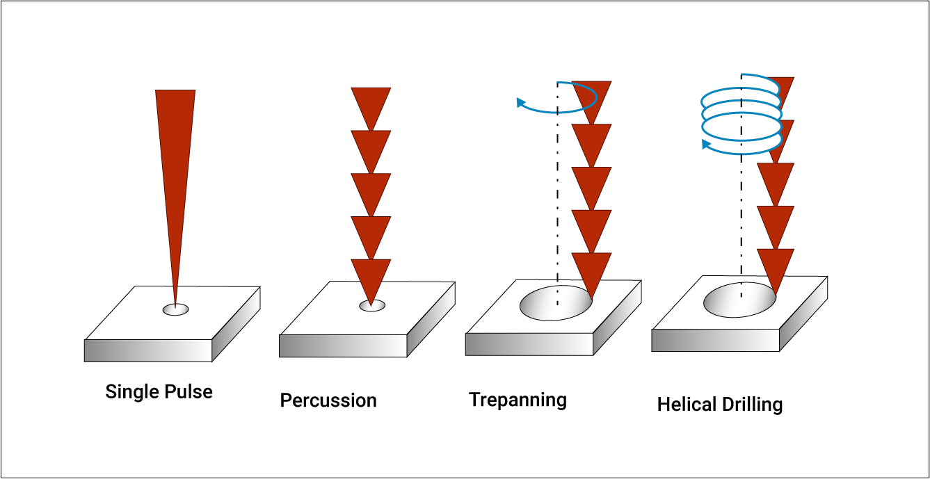
Single-pulse/shot laser drilling
As the name suggests, in single-pulse laser drilling, a single shot of laser beam is fired at the material to create the required hole. In this method, both the source of the laser and the work material is kept static.
Percussion laser drilling
In percussion drilling, a series of laser pulses are shot at the work material repeatedly. During this process, there is no relative motion between the laser beam and the workpiece. This form of laser drilling effectively creates deeper and precise holes with smaller diameters as compared to single-shot laser drilling.
Trepanning

Trepanning is the process in which a laser beam is guided around a predefined locus. This locus is the center of the via to be drilled. It is used in situations where the diameter of the via to be cut is larger than the laser beam diameter. The accuracy of the via is determined by the movement of the beam.
Helical laser drilling
Helical laser drilling is a method in which the laser beam follows a helical path for movement while rotating about its own axis with respect to the workpiece. A dove prism controls the movement of the laser beam.
Which lasers are suitable for drilling small holes?
There are different types of laser machines available that can be used for a variety of purposes. These purposes can be hole creation, etching, depaneling, etc. Out of these, only those machines which can accurately create small holes on the type of materials used for circuit boards should be used as PCB drilling machines.
What is a PCB drilling machine?
A PCB drilling machine drills holes with high precision and accuracy based on the provided data. This data includes the exact position, number, and other parameters of the holes to be drilled.
Types of laser drilling machines
Different types of machines for laser processing are available depending on their operating principles. The most commonly used machines for drilling microvias are CO2 and Nd:YAG lasers. Excimer lasers are also available and are used in the etching of polymers. They are not suitable for the removal of metals.
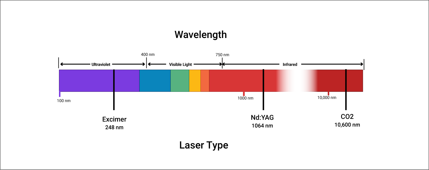
CO2 lasers
Will only ablate dielectric material and not copper.
Carbon dioxide lasers use gas as the lasing medium and emit light in the IR spectrum with around 10.6μm wavelength. These lasers create holes with 50-70μm diameter. CO2 lasers will only ablate dielectric material and not copper. They are one of the high-power lasers available today and are suitable for the drilling of polymers. These lasers have high reflectivity from metal surfaces. They are mostly used in areas where the speed of drilling is of primary importance. For around 80% of microvia drilling, CO2 lasers are used.
Nd:YAG lasers
The lasing medium in the Nd:YAG lasers is solid. Their fundamental emission is in the IR spectrum with a 1064nm wavelength. With non-linear crystals, they emit light in the visible spectrum (532nm) and in the UV spectrum (355 or 266nm). The Nd:YAG lasers can emit up to 100,000 pulses per second. The diameter of the focussed beams of these lasers is 12 to 25μm. For holes with higher diameters, they use the trepanning method.
The Nd:YAG lasers are the most versatile and can be used to drill on different types of materials such as polymers, glass, and metals, etc.
Combination of Nd:YAG and CO2 laser processes
Sometimes, we use a combination of both lasers to get the specific results we want.
An illustration is shown below:
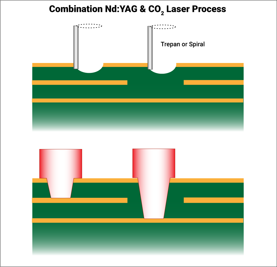
The working procedure of this combination of lasers is explained below:
- Yag is used to remove the top copper which basically creates a stencil for the Co2
- Co2 is used to remove the dielectric material down to the copper landing pad without damaging it
- Co2 leaves an epoxy residue on the capture pad which needs to be removed using a final pass with either the Yag laser or Plasma
Considerations during laser drilling
During laser drilling, there are a few aspects regarding the circuit board that should be considered. Given below are two of the important ones.
Non-homogeneity of the stack-up
The non-homogeneity of the PCB materials used in the stack-up is the main consideration while using lasers. Different materials absorb energy at different rates. For example, FR4 resin absorbs light energy at the same rate as the glass fibers and leaves a clean hole. BT epoxy resin vaporizes at a rate faster than glass and hence leaves glass fibers in the hole.

PCB Material Design Guide
9 Chapters - 30 Pages - 40 Minute ReadWhat's Inside:
- Basic properties of the dielectric material to be considered
- Signal loss in PCB substrates
- Copper foil selection
- Key considerations for choosing PCB materials
Download Now
In situations like these, obtaining complete accuracy with lasers becomes difficult. Therefore, it is recommended to keep the homogeneity of the PCB stack-up as much as possible. If we use materials that have different optical and thermal properties, the way the laser beams react with them will also be different, leading to inaccurate drilling.
The thickness of copper
The minimum thickness of the target copper layer should be twice the thickness of the top copper layer to be penetrated.
Apart from a few challenges that may arise, we can surely say that lasers are the best choice to create microvias in PCBs. Given the ever-increasing demand for reducing the board size and increasing the wiring density, laser-drilled microvias are crucial in PCB manufacturing. Creating diminished holes with extreme accuracy without affecting the integrity of the board is a difficult task. Laser drilling is the best way to manufacture such compact boards.
Want to learn more about laser drilling? Let us know in the comments section.