


Contents

On-demand webinar
How Good is My Shield? An Introduction to Transfer Impedance and Shielding Effectiveness
by Karen Burnham
Signal integrity analysis provides the measurement of the amount of signal degradation when the signal travels from the driver to the receiver. In other words, it signifies the signal’s ability to propagate along PCB traces without distortion.

What is PCB simulation?
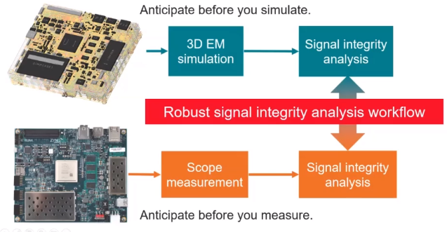
Simulation of a PCB is carried out to understand the actual behavior of the circuit board. It basically increases the efficiency of fabrication by providing a quick preview of how the printed circuit board is going to perform. Simulation (3D electromagnetic simulation) is performed once the PCB layout is ready. This is followed by signal integrity analysis.
Once the board is fabricated, scope measurement and SI analysis are performed. SI analysis is performed twice, once in the layout stage and once after the board is fabricated.
To learn about circuit simulation, read how does circuit simulation work?
How to unlock signal integrity analysis potential?
There are three aspects to be considered here:
- Understand the root causes of SI problems
- Have a realistic virtual prototype
- Rely on dependable PCB manufacturer
Let us see how these three points come together in a PCB design workflow.
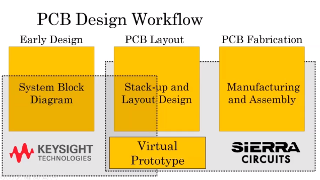
Circuit board design workflow has three main phases. They are early design, PCB layout, and PCB fabrication. The system block diagram is drawn during the early design phase. PCB layout phase has stack-up and layout design. Finally, the manufacturing and assembly of a board are carried out in the fabrication phase. Sierra Circuits and Keysight Technologies provide assistance throughout all these phases. Virtual prototypes are generally sent to the manufacturers before the fabrication process begins.

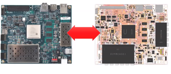
Example of a virtual prototype
A virtual prototype allows the designers to identify and address issues related to signal integrity, thermal management, and manufacturability before the fabrication of the PCB prototype. The below image shows a virtual prototype of Xilinx FPGA ZCU104.
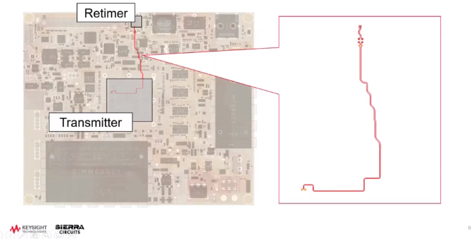
The simulation is carried out by considering a net. Here we consider the signal flowing from the CPU (transmitter) to the HDMI retimer. The signal flow is shown in the image below.
Metrics to anticipate the signal loss
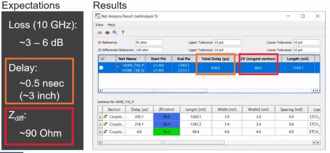
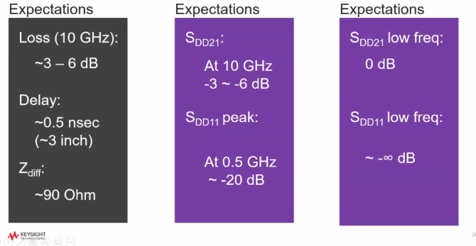
Before we begin the simulation, it is very important for us to anticipate the signal losses. The losses can be manually calculated using loss metrics.
Calculation of signal loss
The length of the trace is about 3 inches and the loss is 0.1 to 0.2 dB/in/GHz. The signal loss can be calculated as shown below:
0.1 x (3 inches) x (10 GHz) = 3 dB;
0.2 x (6 inches) x (10 GHz) = 6 dB
Therefore we can expect a loss of 3 to 6 dB.
Calculation of time delay
We use signal speed in FR4 to anticipate the time delay. That is 6 inches/nanosecond. The time delay can be calculated as shown below:
Time delay = (length of the trace)/(signal speed in FR4);
(3 inches)/ 6 ns = 0.5 ns . The expected time delay is about 0.5 nanoseconds.
Calculation of differential impedance (Zdiff)
We use the impedance rule of thumb to anticipate the Zdiff.
Before we get into that, let us have detailed information on the HDMI traces.
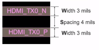
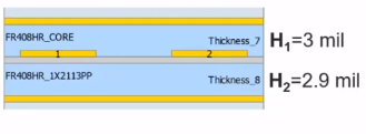
The stack-up says the H1 is 3 mils and the H2 is 2.9 mils. The differential impedance can be calculated using the impedance rule of thumb.
Impedance rule of thumb: If the width over the minimum (H1, H2) is about 1 and the spacing is around 3W then the differential impedance is equal to 100 ohms.
The differential impedance can be calculated as shown below:
Zdiff = 100 ohms if; W / {min (H1, H2)} is equivalent to 1 and S is greater than 3W. Where W is the trace width. Here, the first condition (W/ {min (H1, H2)} is equivalent to 1) is almost satisfied. For the second condition (S should be greater than 3W) to be satisfied, the spacing should be around 9 mils. The spacing in this case is around 4 mils. That means the differential impedance is going to be less than a hundred ohms. Let us assume that the impedance is around 90 ohms.
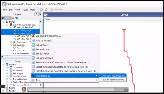
Now, we have all the anticipated values. These values can be cross-verified by performing a quick RapidScan. Follow the below steps to run a 2D RapidScan in Keysight EDS.
- Import the board into the software. Keysight ADS SIPro will show all the nets of the board imported
- Select the HDMI nets (signal propagating from CPU to retimer).
- Right-click and choose the options RapidScan-Z0 > Analyze transmission. The steps are shown in the image below.
Transient analysis is one of the key aspects to ensure signal integrity in your design. To learn more about it, see Transient Analysis for Non-Sinusoidal Signals.
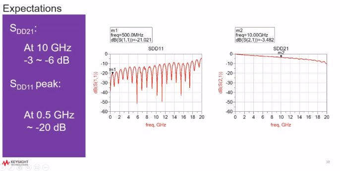
The image below shows the comparison between the expected and actual results of the simulation.
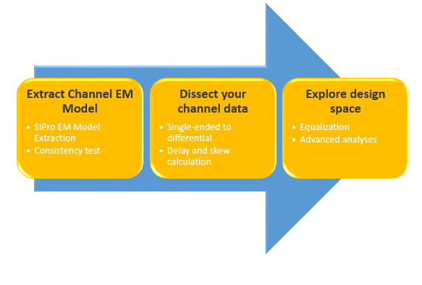
Robust signal integrity simulation workflow
A robust signal integrity workflow includes extracting the channel Electromagnetic (EM) model, dissecting channel data, and exploring design space. The flow chart below shows the robust signal integrity simulation process.

Signal Integrity eBook
6 Chapters - 53 Pages - 60 Minute ReadWhat's Inside:
- Impedance discontinuities
- Crosstalk
- Reflections, ringing, overshoot and undershoot
- Via stubs
Download Now
Extracting the channel EM model
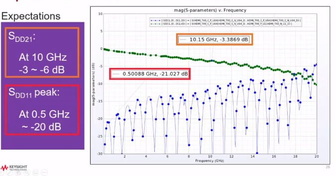
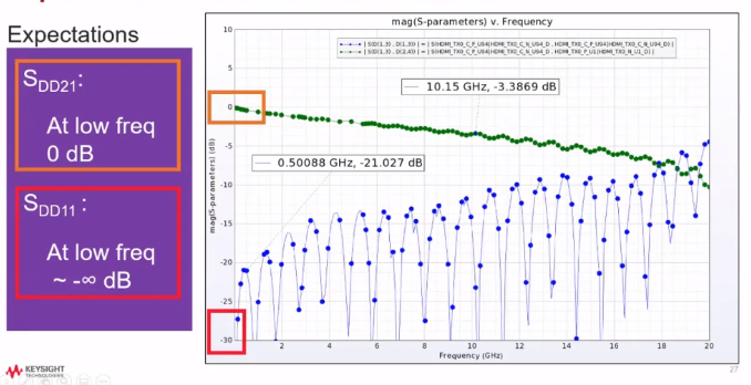
The first step of the simulation workflow is to extract the channel EM model. Before we do that, we need to anticipate the values. We now convert the known values into S parameters. The image below shows the converted values.
The images below show that the expected and the resultant values of S parameters are consistent for low and high frequencies.
Dissect your channel data
The first step is to convert single-ended trace to differential pair. The image below shows the setup to convert single-ended trace to differential pair.
Conversion of single-ended trace to differential pair
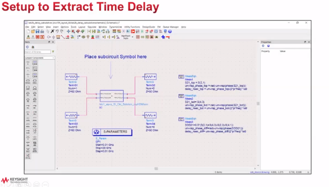
Delay and skew calculations
The setup below can be used to extract the time delay.
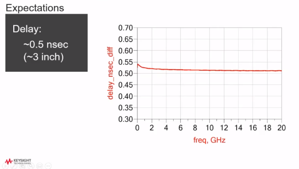
The image below shows that the expected values are consistent with the simulation data.
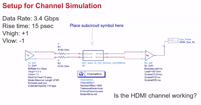
Channel simulation
The channel simulation will use PRBS (pseudo-random binary sequence) to evaluate the signal integrity. The image below shows the setup for the channel simulation.
The comparison between the expected eye diagram and the simulation data is shown below.
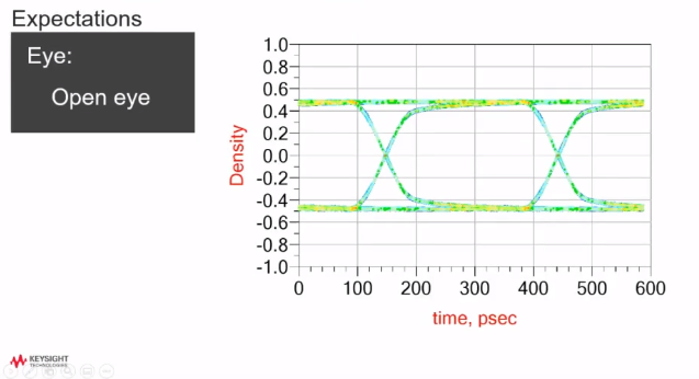
The eye diagram clearly shows that the simulation result has an open eye. Therefore the expectation is consistent with the simulation data.
Explore design space
In this step, we perform equalization and other advanced analyses on the virtual prototype.
Watch the whole webinar to get more practical knowledge of SI analysis. If you want to learn more about any particular aspect of signal integrity simulation then let us know in the comment section.

High-Speed PCB Design Guide
8 Chapters - 115 Pages - 150 Minute ReadWhat's Inside:
- Explanations of signal integrity issues
- Understanding transmission lines and controlled impedance
- Selection process of high-speed PCB materials
- High-speed layout guidelines
Download Now
About The Keysight ADS Team : Advanced Design System is the world’s leading electronic design automation software for RF, microwave, and high-speed digital applications. ADS pioneers the most innovative and powerful integrated circuit-3DEM-thermal simulation technologies used by leading companies in the wireless, high-speed networking, defense-aerospace, automotive and alternative energy industries. For 5G, IoT, multi-gigabit data link, radar, satellite and high-speed switched mode power supply designs, ADS provides an integrated simulation and verification environment to design high-performance hardware compliant with the latest wireless, high speed digital and military standards. Key Benefits of ADS Complete, integrated set of fast, accurate and easy-to-use 3D EM, circuit & system simulators Verification libraries for emerging wireless, automotive, and defense-aerospace standards Supported by leading IC foundry and industry partners


