


Contents

On-demand webinar
How Good is My Shield? An Introduction to Transfer Impedance and Shielding Effectiveness
by Karen Burnham
PCB designers are crucial in developing electronic devices, from smartphones to spacecraft. Circuit board design involves creating detailed schematics that define the layout and connections of electronic components on a board.
Understanding the fundamentals of electronics and mastering design software are crucial stepping stones in the path to learning circuit board design.
In this article, you will learn the educational background and essential skills required to become a proficient PCB designer in 2026.
Highlights:
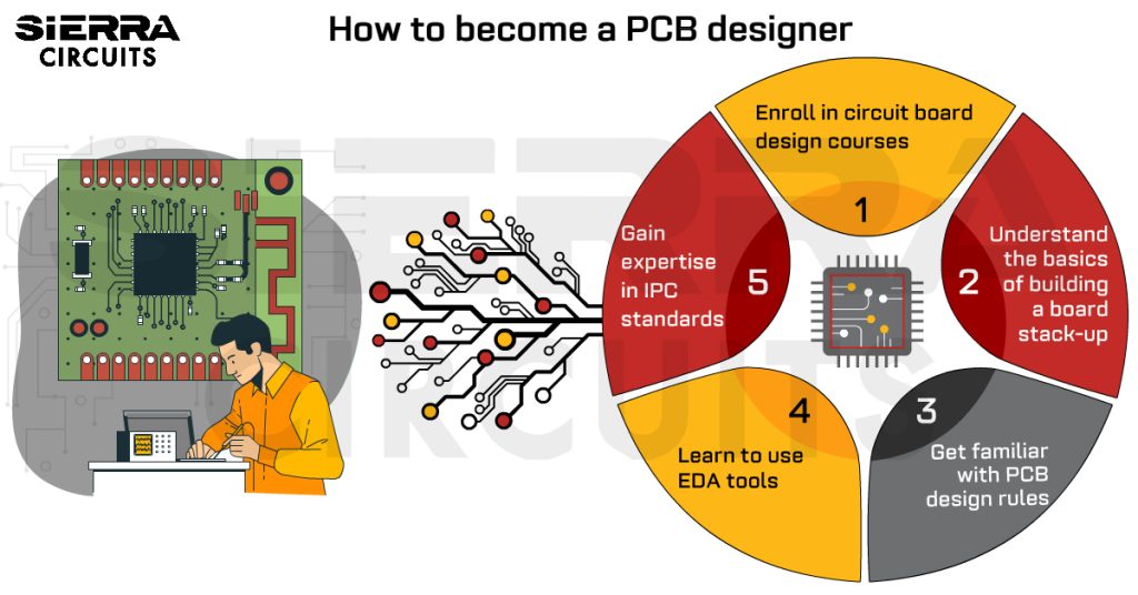
To become a printed circuit board designer:
- Learn how to use circuit board design software like Zuken CR-8000, Altium Designer, Cadence Allegro, KiCad, Mentor Graphics PADS, etc.
- Attain IPC certifications, including CID and CID+, that are well-recognized in the industry.
- Comprehend the basics of building a circuit board stack-up.
- Enroll in specialized courses and certifications covering high-speed boards, RF designs, and signal integrity.
PCB market size- 2017 to 2026
With technological advancements expanding into every facet of our lives, the demand for skilled circuit board designers is at an all-time high in 2026. These individuals play a crucial role in translating technological concepts into reality.
Printed board design market size in the US
According to projections for the financial years 2023 to 2026, the US PCB design services market is set to grow substantially. Starting at US $1.17 billion in 2023, the market is anticipated to reach US $2.14 billion in 2026, reflecting a remarkable compound annual growth rate (CAGR) of 6.4%.

Source: Sierra Circuits’ market research analysis report.
Global printed board market outlook
The printed circuit board market is poised for significant expansion on a global scale. From $66.76 billion in 2021, the market is projected to grow to $93.64 billion by 2026, demonstrating a robust CAGR of 5.8% with an average annual growth rate of 6.5%.

Source: Sierra Circuits’ market research analysis report. To obtain these market insights, we analyzed industry leaders’ annual reports.
This growth trajectory indicates the increased adoption of electronic components across various industries and highlights the escalating demand for PCB designers in the United States.
The printed board design field in the US experienced robust growth by creating approximately 10,500 new job openings in 2024, as per Zippa’s analysis. This demand for designers is expected to sustain a yearly growth rate of 3% from 2018 to 2028. The surge in job opportunities in this niche highlights the increasing importance of skilled professionals in designing and optimizing printed circuit boards.
Roadmap to becoming a PCB designer in 2026

Educational qualifications and certifications to become a PCB designer
Pursue a bachelor’s degree in engineering
A bachelor’s degree in Electrical Engineering, Electronics, or a related field is often a minimum requirement. For specialized expertise, you can opt for a master’s degree in these fields. These degrees provide a solid foundation in the principles of electronics, electrical circuits, and related topics.
Many universities, such as MIT, Stanford, UC Berkeley, Northeastern University, California State University, and Purdue University, offer PCB design courses as a part of their electrical engineering or electronics programs.
A few courses you might have to take to learn more about circuit board basics while pursuing engineering include:
- Circuit theory, simulation, and design
- Digital and analog electronics
- Electromagnetics
- Power systems
- Circuit board layout
- RF antennas and design
Get enrolled in specialized PCB design courses
Several institutions and online platforms offer printed circuit board design courses and certifications.
Online circuit board training platforms
- Udemy: They offer various courses on circuit board design, ranging from beginner to advanced levels. Here is a list of their highest-rated courses:
- Crash course electronics and PCB design
- PCB design using OrCAD/Allegro from basics to expert level
- Circuit design, simulation, and PCB fabrication bundle
- Advanced hardware and PCB design masterclass
- Learning complete PCB design: From an idea to a product
- Coursera: You can explore courses from institutions like Johns Hopkins University or the University of California, Irvine. The most popular courses they offer are:
- Designing hardware for Raspberry Pi projects
- Powering your home projects with Raspberry Pi specialization
- edX: You can take courses from reputable institutions like MIT on edX. A few courses they provide include:
- MITx’s circuits and electronics XSeries program
- NUS: Circuits for beginners
Offline circuit board training platforms
- PCEA: The printed circuit engineering association was driven by prominent figures in printed circuit engineering and manufacturing, such as Rick Hartley, Mike Creeden, Susy Webb, Stephen Chavez, and Gary Ferrari.
It offers a five-day course by industry experts Michael Creeden and Tomas Chester. The course covers the fundamentals of circuit boards, documentation, manufacturing preparation, and advanced electronics.
After completing the workshop, you can pursue an additional CPCD (certified printed circuit designer) certification.
- EPTAC offers online and offline training programs and certifications in electronics manufacturing, including PCB design.
- IPC designer certification (CID)
- IPC advanced designer certification (CID+)
Further, look for advanced courses covering topics such as high-speed design, microwave, radio frequency design, power, and signal integrity. These courses will help you specialize in specific areas.
PCB layout design software
Proficiency in layout design software is crucial. Popular tools include Altium Designer, Cadence Allegro, Zuken CR-8000, Mentor Graphics PADS, etc. Consider taking courses specific to the software you’ll be using. Check for training programs that the tool’s developer or authorized training partners provide.
IPC certification
IPC, the association connecting electronics industries, offers various PCB design and assembly certifications. IPC’s certified interconnect designer (CID) and IPC CID+ (advanced) are well-recognized certifications that will help you establish your career in the industry.
You can register for these courses and attend training from an IPC-authorized training center such as EPTAC. After successfully passing the written exam, you will receive the IPC CID certification. The CID+ program is designed for experienced designers who have completed the CID certification.
Boost your skills by reading PCB design books
While hands-on experience is essential, understanding the concepts and best practices through design books will equip you with a strong knowledge base to excel in this industry.
Here are a few books suggested by Rick Hartley, an EMI and signal integrity expert:
- Fast Circuit Boards: Energy Management by Ralph Morrison
- PDB Design for Real World EMI Control by Bruce R Archambeault
- Electromagnetic Compatibility Engineering by Henry W.Ott
- Lee W. Ritchey
- Signal and Power Integrity Simplified by Eric Bogatin
Further, Eric Bogatin’s “Practical Guide to Transmission Line Design and Characterization for Signal Integrity Applications” can also be useful for aspiring printed board designers.
For insights into designing PCBs with signal integrity, download the Signal Integrity eBook.

Signal Integrity eBook
6 Chapters - 53 Pages - 60 Minute ReadWhat's Inside:
- Impedance discontinuities
- Crosstalk
- Reflections, ringing, overshoot and undershoot
- Via stubs
Download Now
9 essential skills to become a proficient PCB designer in 2026
Designing a circuit board is a crucial part of creating electronic products. It involves translating a PCB schematic into a physical board.

Let’s break down the essential skills needed for printed circuit board design:
1. Solid grasp of basic electronics
Knowing basic electronic principles, circuit board components, and their behavior is crucial. You must also understand the basic physics and mathematics concepts to calculate parameters like impedance, signal timing, and power distribution.

Build a solid foundation in electronic fundamentals by learning more about the basic electronic components.
2. Understanding circuit board fundamentals
As a PCB designer, you need to know the terminologies, tools, technology, and basic design principles involved in the circuit board manufacturing process. Understanding the basics, such as what a printed circuit board is and how traces, pads, and power planes work, can help you perform your job more efficiently.
PCB design is an artistry, says Rick Hartley. His advice to all aspiring PCB design engineers and beginners is not just to design circuit boards but to constantly learn by talking to manufacturers and fabricators assemblers. Learn about transmission lines and energy movement, high-speed design, noise control, EMI control, and how to reduce the cost of the product.
To understand the basics of circuit board design, read mastering the art of PCB design basics.
3. Proficiency in building PCB stack-up
It is vital to understand how to arrange the layers of your PCB stack-up, balance it, and decide the number of laminations. This includes decisions about signal layers, power planes, and ground planes, considering factors like impedance control and electromagnetic interference.

The knowledge of building a PCB stack-up, combined with design concepts like external noise reduction and radiation minimization, is vital for designing effective multilayer circuit boards.

4. Skilled in using printed board design tools
Proficiency in electronic design automation tools like Zuken CR-8000, Altium Designer, Cadence Allegro, KiCad, and Mentor Graphics PADS is necessary for aspiring circuit board designers, as their usability extends beyond creating PCB layouts.
If you’re still early in your educational journey, consider utilizing open-source PCB design software to grasp the workflow of board design. However, when aiming for a professional career, it becomes evident that open-source EDA programs are not widely used, and a more robust EDA tool is necessary.

Read 13 most used layout design tools to get insights into commonly used EDA tools.
5. Expertise in IPC standards
Mastering IPC standards is your key to building an error-free circuit board. They cover various aspects, including design, materials, and manufacturing processes.
IPC-2221: Generic standard on printed board design: Provides guidelines on the design of printed boards and includes considerations for material selection, conductor spacing, and thermal management.
IPC-2222: Sectional design standard for rigid organic printed boards: Focuses on specific design requirements for rigid PCBs, covering aspects like layer stacking, conductor thickness, and dielectric materials.
IPC-2223: Sectional design standard for flexible printed boards: Outlines design guidelines specifically for flexible printed boards, addressing aspects such as bending radius, material selection, and circuit layout.
To get more insights into IPC for flexible boards, read IPC guidelines and basic testing for Flex PCBs
IPC-2226: Sectional design standard for HDI printed boards: Pertains to the design considerations for HDI boards, emphasizing aspects like microvia design, layer buildup, and fine-line geometries.
IPC-2152: Standard for determining current-carrying capacity in PCB design: Provides guidelines for determining the current-carrying capacity of conductors on printed boards, addressing factors such as temperature rise, conductor width, and thermal conductivity.
IPC-A-600: Acceptability of printed boards: Establishes the criteria for assessing the quality and acceptability of bare printed boards, including requirements for surface finish, hole plating, and conductor spacing.
IPC-6012: Qualification and performance specification for rigid printed boards: Details the performance and qualification requirements for rigid PCBs, covering criteria for base materials, conductor thickness, and plated-through holes.
Both IPC-6012 and IPC-A-600 are applicable to rigid boards. To learn the difference, read IPC-6012 or IPC-A-600: Which standard should you use?
IPC-6013: Qualification and performance specification for flexible printed boards:
Outlines performance and qualification criteria for flexible PCBs, covering material properties, dynamic flexing, and adhesion.
IPC-6018: Qualification and performance specification for high frequency (microwave) printed boards:
Addresses the unique requirements for high-frequency printed boards, including dielectric constant, loss tangent, and conductor geometry.
IPC-7711/7721: Rework, modification, and repair of electronic assemblies:
Guides PCB designers on standards for rework and repair, covering procedures for removing and replacing components and modifying assemblies.
IPC-7351: Generic requirements for SMD and land pattern standard: This standard specifies guidelines for surface-mount device (SMD) land patterns, aiding designers in creating accurate component footprints.
Awareness of different design rules of IPC class 2 and class 3 can also be useful in your career as a PCB designer. Remember that these standards are regularly updated, so staying current with the latest revisions is essential for maintaining industry best practices.
6. Familiarity with PCB design rules
Knowledge of design rules ensures that the circuit board meets manufacturing and performance requirements. This includes trace width, spacing, and other layout constraints. All PCB design organizations follow certain standard design principles and guidelines, as it enables them to design and deliver accurate circuit boards to their clients. Here are a few design guidelines you must remember while designing a board.
- Material selection: Gain insights into choosing appropriate PCB materials, considering factors like dielectric constant, thermal conductivity, and substrate properties to meet specific design requirements.
- PCB layer stack-up: Explore the complexities of building a layer stack-up and master the arrangement of signal layers, power planes, and ground planes. This knowledge is essential for achieving desired electrical performance and manufacturability.
- Design rule checking (DRC): Understand the importance of a circuit design’s compliance with a set of predefined rules or constraints. These DRC rules typically cover aspects such as trace widths, spacing, minimum clearances, hole sizes, and other design parameters necessary for the successful fabrication and assembly of the board.
- Component placement guidelines: Learn the art of strategically placing components on a PCB for optimal functionality.
- Power distribution and grounding: Grasp the principles of effective power distribution and grounding to avoid voltage drops, reduce noise, and create a stable electrical environment on the printed circuit board.
- Signal integrity considerations: Understand the critical aspects of maintaining signal integrity, including considerations for trace length, impedance control, electromagnetic interference, and electromagnetic compatibility, and minimizing signal crosstalk.
- Circuit board thermal management techniques: Learn how to effectively manage heat on a PCB, including placing thermal vias and heatsinks.

- Design for testing: Understand DFT strategies to facilitate ease of testing and debugging, incorporating features like test points and access to critical nodes for troubleshooting.
- Design validation and simulation: Explore using simulation tools to validate your designs before production, ensuring they meet performance expectations and identifying potential issues early in the design process.
- Design for manufacturability: Familiarize yourself with DFM principles to create functional, easily manufactured, cost-effective designs. Consider factors like component spacing, trace width, and spacing, via/pad size, drill size, and solder mask clearances.
To learn how to design a cost-efficient PCB without board respins, download the Design for Manufacturing Handbook.

Design for Manufacturing Handbook
11 Chapters - 96 Pages - 90 Minute ReadWhat's Inside:
- Annular rings: avoid drill breakouts
- Vias: optimize your design
- Trace width and space: follow the best practices
- Solder mask and silkscreen: get the must-knows
Download Now
7. Well-versed with the design review process flow
Learning the PCB review process is essential for a smooth circuit board design process. You must follow a detailed design review process to ensure high-quality designs for any manufacturer or organization. Check the layout for faults and areas of improvement to ensure it meets the design objectives.
The typical three-stage review process includes an initial designer review, followed by a hardware engineer review, and a final assessment by a qualified engineer/consultant. A systematic design review helps catch errors and improve the overall design. Being open to feedback and learning from reviews is crucial for continuous improvement.

8. Knowledge of PCB manufacturing and assembly processes
Designers do not necessarily have to be experts in setting up a PCB manufacturing plant. However, it’s a value addition to be familiar with the fabrication process and its impact on circuit board layout design. Knowledge of PCB manufacturing and circuit board assembly can help you anticipate and prevent circuit board failures during fabrication and assembly.
For step-by-step guidance on getting your first prototype fabricated, read how to get your first PCB manufactured.
9. Soft skills required as a designer
Attention to detail: Precision is critical in circuit board design. Small errors can lead to significant issues, affecting the final product’s functionality, performance, and manufacturability.
Problem-solving skills: PCB designers often encounter challenges with signal integrity, thermal management, or manufacturability. Strong problem-solving skills are essential to identify and address these issues effectively.
Teamwork: Printed circuit board design requires collaboration with engineers, including electrical engineers and production teams. Collaboration between PCB designers and electrical engineers leads to creative solutions and quicker design times.
Communication skills: Effective communication is essential when working in a team. Collaborating with other engineers, manufacturers, and stakeholders requires clear and concise communication to ensure everyone is aligned on design goals and specifications.
To know more, read how modular PCB design method simplifies complex layouts.
Staying current in the circuit board industry
The PCB industry constantly evolves due to rapid technological breakthroughs in multiple fields, from consumer electronics to aerospace and defense applications. Hence, continued learning is essential to stay current on the latest tools, materials, and techniques.
Lee Ritchey, a pioneer in high-speed boards who designed a radio for the Apollo program at NASA right out of college (seven of those radios may still be on the moon right now) and put the very first transistor on the moon, aptly advises new designers,
“Do not stop learning as the PCB industry is not static “
Standards and regulations in the electronics industry can change. Hence, staying informed about these updates is crucial to ensure your designs comply with industry standards. This can be done by:
- Learning about emerging technologies: As new technologies emerge, such as IoT (Internet of Things), medical electronics, and wearables, staying current with these trends can open up new opportunities for PCB designers in 2026.
- Flexible PCBs: Crucial for applications like wearables, foldable devices, and medical implants, flexible boards provide great design flexibility.
- Ultra HDI designs: This is particularly beneficial in various technological applications where enhanced connectivity, miniaturization, and advanced signal integrity are critical, such as mobile devices, data centers, aerospace, medical devices, and wearables.
- IoT integration: PCBs must now accommodate heightened connectivity demands, low-power requirements, and increased data flow, especially in interconnected systems like smart homes and cities.
- AI and automation: Cutting-edge tools leverage machine learning to optimize circuit board layouts, predict flaws, and streamline the overall design and manufacturing processes.
- 3D printing: This technology shows promise for producing on-demand multi-layer PCBs, significantly enhancing efficiency in both prototyping and production. Traditional prototyping methods can be expensive and time-consuming. 3D printing reduces material wastage and speeds up prototyping, saving costs.
You can subscribe to a few well-known PCB design magazines, like Design007 and Printed Circuit Design & Fab, which will give you a heads-up on the changes in the industry.
- Professional development: Attending Sierra Circuits’ webinars and seminars, industry conferences, workshops, and networking events provides opportunities to learn from experts, exchange ideas, and stay connected with the broader PCB design community.
For instance, engaging with the Institute of Electrical and Electronics Engineers (IEEE) community and becoming a member of the International Society for Hybrid Microelectronics (ISHM) offers a rich platform for professionals in electrical engineering, electronics, and related fields to enhance their expertise.
- Skill diversification: Expand your skill set beyond basic circuit board design, such as learning about embedded systems, FPGA programming, or software-defined electronics, to become a versatile and in-demand professional.
For more information on embedded passives, read how to design a PCB with embedded components.
Technological advancements that boost the demand for PCB designers
Internet of things
According to Deloitte’s analysis, the global market for IoT and connected devices, including hardware and software, was worth US $800 billion in 2023. This emphasizes the critical need for reliable and well-designed circuits and the growing need for more capable designers who can achieve this.
Wearable technology
The demand for compact devices like smartwatches and fitness trackers is experiencing significant growth. In 2022, the wearable technology market was valued at US $139 billion. With a growing CAGR of 18.5%, by 2030, the wearables market could be worth more than US $540 billion, as per ResearchGate’s prediction.
Medical electronics
Due to the pandemic in 2020, the need for remote medical services and fast diagnostics increased the demand for medical PCBs. The global market size for medical electronics surged in 2021 to US $586 billion, as reported by TTI.
The demand for expertise in designing cutting-edge printed circuit board technologies is growing steadily. As the use of advanced electronic devices has become a routine part of our daily lives, the increasing demand for products makes the future of electronic design appear highly promising.
However, the current shortage of skilled designers and manufacturing professionals, primarily due to the imminent retirement of many experienced designers, poses a challenge. The industry’s response is new onboarding initiatives and a surge in job opportunities, which make circuit board designing a highly promising career.
Designing a high-quality, manufacturable circuit board requires expertise in stack-up design, EDA tools, and IPC standards. Let our PCB design services guide you from concept to product. Get a quote for your PCB design today!
You can book a meeting with our experts or call us at +1 (800) 763-7503.

Key takeaways:
- The US PCB design services market is projected to grow from US $1.17 billion in 2023 to US $2.14 billion in 2026, with a CAGR of 6.4%.
- A bachelor’s degree in Electronics and Electrical Engineering or related fields is often a minimum requirement, with options for specialized expertise through master’s degrees.
- Universities like MIT, Stanford, UC Berkeley, and others offer circuit board design courses as part of their programs.
- Advanced courses covering high-speed board design, RF design, power, and signal integrity are recommended for specialization.
- To stay updated on PCB design industry trends, it is crucial to participate in professional development, industry conferences, workshops, and networking events.
- Knowledge of IPC standards, EDA tools, and circuit board design rules is important for becoming a circuit board designer in 2026.
- Soft skills like attention to detail, problem-solving, teamwork, and communication are important.
- It is crucial to be aware of emerging technologies like flexible boards, ultra-HDI designs, IoT integration, AI, automation, and 3D printing.
Need assistance in designing your first circuit board? Post your queries and get them answered on our PCB forum, SierraConnect.

About Pooja Mitra : Pooja Mitra is an electronics and communication engineer. With an experience of over three years in the PCB industry, she creates industry-focused articles that help electrical and PCB layout engineers.


What are the key differences between academic projects and real-world PCB design challenges, and how can recent graduates bridge the gap to ensure readiness for professional roles?
What role do internships, co-op programs, or freelance projects play in helping recent graduates gain practical experience and build a portfolio to enhance their job prospects in PCB design?
An absolutely critical one. Companies won’t hire recent graduated students who don’t have industry experience. Especially in hardware and printed circuit board design.
For such a skill as PCB design, only experience matters and those are the candidates that get hired the most (I deal with multiple EEs and their lived experiences and persistent rejections happen all the time, simply because someone had sufficient PCB experience while they had very little or none at all).
So a portfolio of some kind is essential. Mandatory I would say.
The key differences between academic projects and real-world PCB design challenges lie in complexity, constraints, and practical considerations. Academic projects often focus on theoretical concepts with simplified requirements, whereas real-world challenges involve multifaceted constraints like cost, manufacturability, and performance optimization.
Recent graduates can bridge this gap by gaining practical experience through internships, freelance projects, or industry collaborations.
Additionally, staying updated with industry-standard tools, learning project management methodologies, networking with professionals, attending industry events, and seeking mentorship can enhance readiness for professional roles.
I recently graduated with a bachelor’s degree in Electrical Engineering and have been exploring various career opportunities. I have an upcoming interview for a PCB designer position, which got me thinking about how to become a PCB designer and whether it’s the right path for me. I have some experience in PCB design and find it interesting, but I’m unsure if this role would fully utilize my EE degree.
The job description doesn’t specifically require an EE degree—it’s more of a “nice to have” rather than a strict necessity. This makes me wonder if pursuing a career in PCB design is the best use of my skills and education. Ideally, I’m looking for a role that is very hands-on, working directly with hardware, doing lab work, learning about circuit design, testing, etc. I’m worried that a job focused on PCB design might not allow me to deepen my core EE knowledge. However, I could be wrong.
On the other hand, the opportunity is with a highly reputable company, which would look great on my resume and could open doors in the future.
I’m also curious about the salary prospects—does a career in PCB design typically offer competitive pay compared to other EE roles? I’m also considering my student loans, so that’s a significant factor. Any advice or insights would be appreciated!
A job title, especially in engineering, can encompass a wide range of responsibilities depending on the company’s size, structure, and specific needs. For instance, the role of a “PCB designer” can vary significantly from one company to another. Here are some points to consider:
Diverse Responsibilities Across Companies: In many medium to large-sized companies in the USA, a PCB designer’s role could range from purely layout-focused tasks to more integrated responsibilities that involve circuit design, component selection, and coordination with other engineering teams. In smaller companies, a PCB designer might wear multiple hats, taking on tasks that, in larger organizations, would be divided among several specialists.
Engineer vs. PCB Designer Roles: Typically, in larger companies:
Design Engineers (Digital, Analog, RF, etc.): These engineers focus on designing and simulating circuits, selecting critical components, and creating the initial schematics. This is likely where you’d be applying more of your core EE knowledge.
PCB Designers: These roles often focus on translating the schematics into a physical layout, taking into account mechanical constraints, production requirements, and other considerations. While this might seem less “EE-focused,” it’s crucial for ensuring that the design can be effectively manufactured and performs reliably in the real world.
Understanding how to become a PCB designer can also vary depending on the company and industry. While the PCB designer role may not always require an EE degree, having one could provide you with a broader understanding of the design implications and allow you to contribute more effectively to cross-disciplinary discussions. It might also position you well for advancement into roles that blend design and layout responsibilities or move into more senior engineering or management positions.
Even in a PCB design-focused role, there are opportunities to deepen your understanding of signal integrity, electromagnetic compatibility, and thermal management—areas that are highly relevant to an EE background. Engaging with these aspects of PCB design can help you develop a more comprehensive engineering skill set.
Considering that the opportunity is with a reputable company, the experience and connections you gain could open doors to other roles that better align with your interests. The salary for PCB designers can be competitive, but it may vary based on location and the company’s size. If you’re concerned about student loans, it’s worth looking at the full compensation package and considering the long-term potential of working at a well-known company.