


Contents

On-demand webinar
How Good is My Shield? An Introduction to Transfer Impedance and Shielding Effectiveness
by Karen Burnham
Electronics is at its peak with the advent of digitization. The components used in electronic equipment may experience certain failures during their operational life.
Common electronic component failures include mechanical, thermal, environmental, electrical stress, packaging, and aging. These defects interfere with the device’s functioning. To deliver a reliable product, it is essential to identify, resolve, and prevent such failures.
PCBs comprise numerous components, including through-hole components and surface-mount devices (SMD). Defects may arise during manufacturing, assembly, and shipping for several reasons. Continuous improvement should be focused on the areas prone to failure.
Check out our PCB component sourcing and stocking services to get your electronics to market fast!
What is electronic component failure?
Electronic component failure occurs when a component does not function or perform as expected. It eventually damages the product. These defects may result in a complete breakdown or degradation in the device’s performance.
It is crucial to perform root-cause analysis to find out the failure modes of components. This research requires some information that includes:
- Circuit board design data, including dimensions, stresses, loads, etc.
- Parts, material, and process specifications.
- Manufacturing process reports involving chemical analyses, mechanical properties, inspections, and performance testing.
- Information related to working environments.
- Maintenance record comprising vibration analysis and previous failures.
All this data will assist in the failure modes and effective analysis of a board.

Common reasons for electronic component failure
Component failures can be caused by mechanical, thermal, environmental, electrical, packaging, or aging factors. It is essential to know all the details about these causes.
Mechanical failure
Mechanical failure in a circuit board includes elastic and plastic deformation, fatigue fracture initiation and propagation, brittle fracture, warpage, and creep and creep fracture.
Elastic and plastic deformation
Deformation is simply the distortion that can change the shape and size of an object. It is of two types: elastic and plastic. Elastic deformation is temporary and goes away after the removal of external forces that cause stress and alteration.
However, plastic deformation is permanent and retains the distortion even after removing external forces that generate stress. PCBs comprise copper foil, resin, glass cloth, and other materials having different chemical and physical characteristics.
Pressing these board materials together sometimes results in deformation. Apart from this, mechanical cutting (V-scoring), wet chemical processes, and high temperature also induce deformation.
Brittle fracture
A brittle fracture is a sudden failure that occurs when equipment rapidly cracks under stress. In such situations, the material shows no sign of degradation or breakage.
This type of failure occurs at the soldered joints in circuit boards. These fractures develop due to tensile stresses in the components during assembly, testing, and transport. Additionally, these fractures exist because of exposure to shocks, vibrations, and thermal excursions.
Implement embedded passives to avoid solder joint failures. To learn more, see how to design a PCB with embedded components.
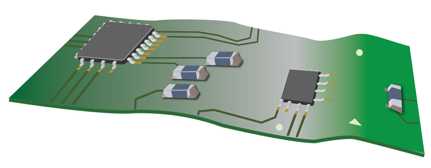
Warpage
Warpage is the twisting or bending of a device that deviates from its original shape due to heat and moisture. PCB warping changes the profile of the board during the reflow soldering cycle.
Warpage can be caused by unbalanced layers during board design, thermal expansion during soldering (due to different material properties), and the weight of components, heat sinks, or shields.
Creep
A creep is a time-dependent deformation resulting from an increase in temperature and constant pressure. The failure resulting from creep is known as creep fracture.
Surface finishes generate creep corrosion. As per the RoHS directive, the electronics industry has to focus on lead-free surface finishes. One cost-effective option is immersion silver, but it is more likely to cause creep.
ENIG (electroless nickel immersion gold) and OSP (organic solderability preservative) possess a low risk of creep. In a harsh atmosphere, creep failure is a growing hazard. Nowadays, researchers are investigating advanced lead-free finishes to mitigate this risk.
Fatigue
Fatigue is the initiation and development of cracks in a material as a result of cyclic loading. In populated boards, solder fatigue is a critical failure.
Inconsistent CTE is the fundamental cause of solder fatigue. CTE determines the contraction and expansion of the material during temperature deviations.
Soldering low-CTE components to low-CTE boards and high-CTE components to high-CTE boards is a good practice. If the CTE is mismatched, solder fatigue eventually forms because of thermal and diurnal effects.

PCB Material Design Guide
9 Chapters - 30 Pages - 40 Minute ReadWhat's Inside:
- Basic properties of the dielectric material to be considered
- Signal loss in PCB substrates
- Copper foil selection
- Key considerations for choosing PCB materials
Download Now
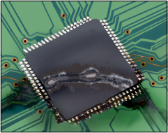
Thermal failure
Thermal failure occurs when the component is heated above its critical temperatures, such as the glass transition temperature (Tg), melting point, or flashpoint. Tg is the temperature at which the base material changes from a rigid to an elastic state.
Substrates decide the Tg value of the circuit board. If the operating temperature exceeds the Tg, it will result in thermal failure, leading to component burning.
For thermal failure analysis, see 12 PCB thermal management techniques to reduce heating.
Environmental failure
Environmental failure results from the entry of foreign objects, moisture, dust, power surges, and exposure to heat.
Vibrations are adverse to populated boards, especially in class 3 products. To know more, see how vibrations in space vehicles affect PCBA.
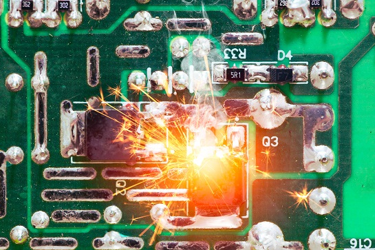
Electrical stress failure
The causes of electrical stress failure include electrostatic discharge (ESD), surface breakdown, dielectric failure, overvoltage, and surface trapping.
ESD
Extreme electrical stress causes ESD that results in catastrophic failure, permanent parameter variation, and hidden damage. This might occur because of high current density, high electric field gradient, and localized heat formation.
PCB assemblies are susceptible to ESD when they come in contact with any charge-carrying object. Depending on the electromotive force between the two and their distance from each other, ESD is most likely to occur when the two are in close proximity.
Dielectric failure
Dielectric failure describes an electric breakdown within a solid insulator placed between two conductors. It is often associated with the puncture or decomposition of the insulation material.
Any material will fracture or puncture at some point when exposed to a high voltage gradient. Material (thickness and quality of sample) and environmental (temperature and humidity) factors influence this level.
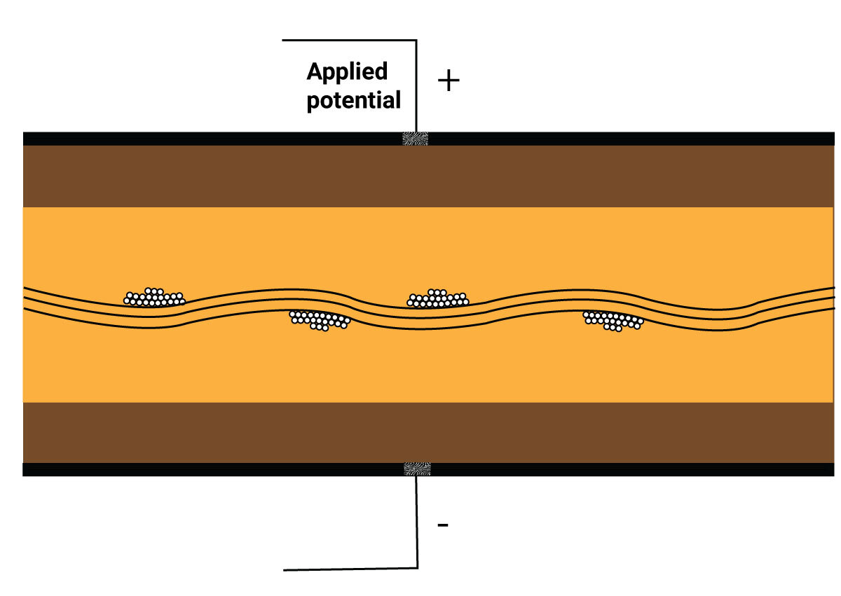
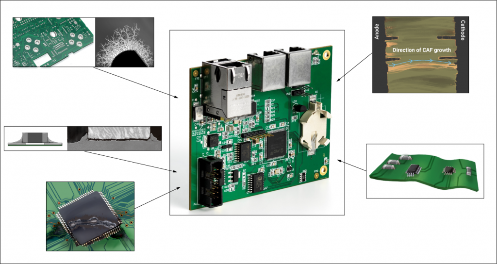
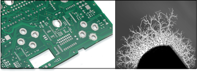
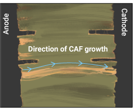
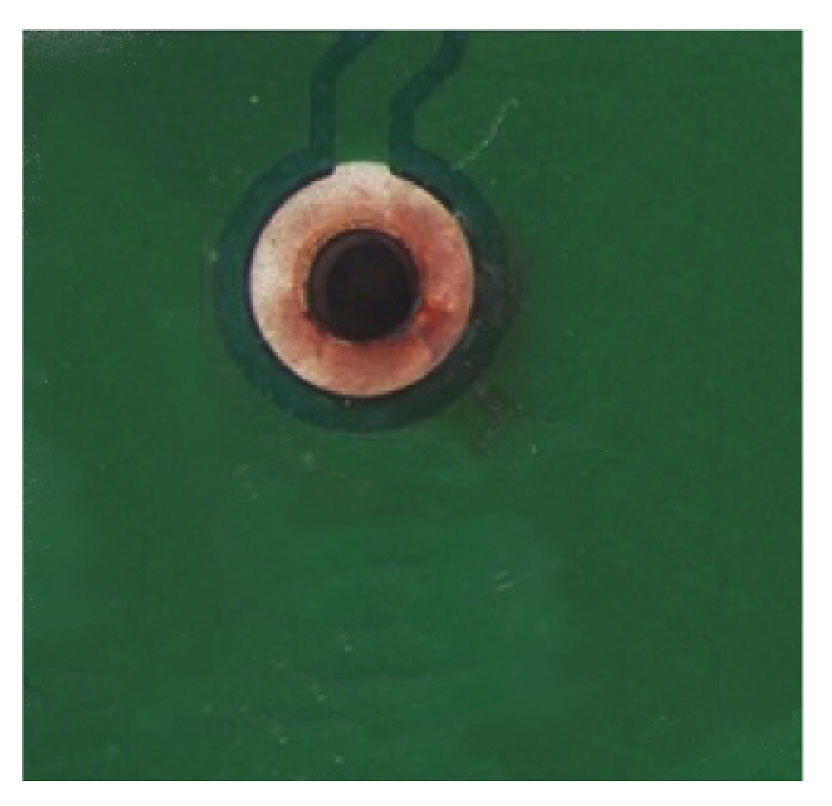
Conductive anodic filaments
Boards may develop conductive anodic filaments (CAFs) along the fibers of the composite material. During the via plating, metal is injected into an exposed surface, where it migrates due to ions, moisture, and electrical potential.
Poor glass-resin bonding and PCB drilling damage are the contributors to such failures. Due to thermal expansion differences between fibers and matrix, the bond weakens after soldering.
Lead-free solders require a higher soldering temperature, which increases the probability of CAFs.
Packaging failure
Packaging is often the cause of breakdowns in many electronic parts. It acts as a barrier between electronic components and environmental influences.
Thermal expansion results in mechanical stresses that damage materials. Aggressive chemicals and humidity may cause corrosion. Excessive thermal stress can overstress wire bonds, causing the connections to loosen, chips to crack, or packaging to break.
The effects of humidity and subsequent high-temperature heating may also cause cracks, leading to mechanical damage. Bonding wires can be cut and shortened during encapsulation.
Aging failure
Each component has a limited operational life. If it operates beyond this point, the possibility of breakdown due to mechanical fatigue will increase.
Through a component lifecycle, its availability advances along various stages. The cycle ends when the component’s production stops.
As a result, parts sourced during this end-of-life (EOL) stage may be outdated and do not meet the latest performance specifications. Thus causing them to fail prematurely.
To understand discrete component failures, read common errors encountered in discrete components.
Methods to determine component failures
It is possible to identify defects with several tests. Failure analysis helps to understand the faults and their prevention, which improves both the production and assembly processes. Here are a few important ones:
Solderability test
Solderability defines the wetting of a metal or metal alloy surface by solder under minimum adequate conditions. Usually, the board manufacturing process itself causes assembly difficulties.
This failure is due to problems associated with oxidation and improper application of the solder mask. To avoid this, check components and pad solderability to ensure the robustness of the surface. It also helps to develop a reliable solder joint.
This testing assesses the strength and wetting quality of the solder by replicating the contact between the solder and the material. It determines the wetting force and the duration from contact to wetting force formation. Moreover, it identifies the cause of the fault. Applications of solderability testing include:
- Evaluation of solder and flux
- Circuit board coating evaluation
- Quality control
Understanding various surface conditions and the testing method’s adequate requirements is crucial to effectively utilize this testing.

Contamination test
Contamination induces various problems, such as corrosion, metallization, and degradation. The circuit board has to go through aggressive chemical solutions within its lifecycle. Such chemicals include etching liquid, fluxes, electrolytic solutions, etc. It is necessary to perform cleaning after the application of these chemicals.
Contamination testing calculates the number of ionic contaminants present in the sample. This process involves immersing the circuit board into a sample solution.
This solution dissolves the ionic impurities that change the composition of the solution and the values. Then, by comparing the actual level with the standard level, it is possible to analyze the severity of the contamination. There should be a focus on the cleaning process to avoid the risks of failures.
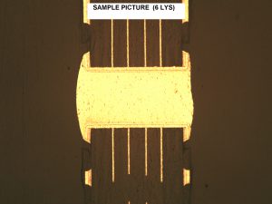
Micro-sectioning test
The micro-sectioning test, also known as cross-sectioning, inspects the following:
- Component defect
- Shorts or opens
- Thermo-mechanical breakdown
- Solder reflow processing failures
- Analysis of raw materials
In this method, a two-dimensional slice is cut out of a sample, which reveals the board’s features. The micro-sectioning analysis is a destructive testing method that provides an accurate way to separate electronic components and remove them from the sample.
Then, it is placed in epoxy resin for curing and solidifying. Later, using an abrasion technique, the component is removed and then polished until it is reflective. This test involves a comparison of this sample with the functioning part.
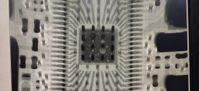
Automated X-ray inspection (AXI)
Automated X-ray inspection (AXI) determines hidden defects related to ICs and BGAs in PCBs. This method accesses internal geometries and structural compositions. The following errors can be detected using this method:
- Soldering defects like opens, shorts, solder bridges, solder voids, excess and insufficient solder, and poor solder quality.
- Component defects like lifted lead, missing component, and misplaced component.
- BGA errors, including BGA shorts and open circuit connections.
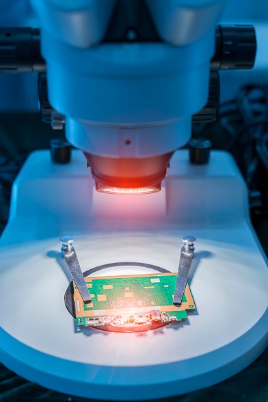
Surface imaging method
One of the most popular testing methods for finding problems related to soldering and assembly is optical microscopy, or the surface imaging method.
The technique is popular due to its efficiency and accuracy. It uses a high-power microscope with visible light. This microscope features a small depth field and one-plane view and can reach a magnification of 1000X. It can verify improper construction, which causes stresses that expose flaws in some cross-sections.
Incorporating an appropriate DFT can mitigate the risk of component collapse and alert the designer. If you have any further questions about common electronic component failures, please let us know in the comments section. Download our design guide to understand assembly aspects for a better design.

PCB Design for Assembly Handbook
6 Chapters - 50 Pages - 70 Minute ReadWhat's Inside:
- Recommended layout for components
- Common PCB assembly defects
- Factors that impact the cost of the PCB assembly, including:
- Component packages
- Board assembly volumes
Download Now


