


Contents

On-demand webinar
How Good is My Shield? An Introduction to Transfer Impedance and Shielding Effectiveness
by Karen Burnham
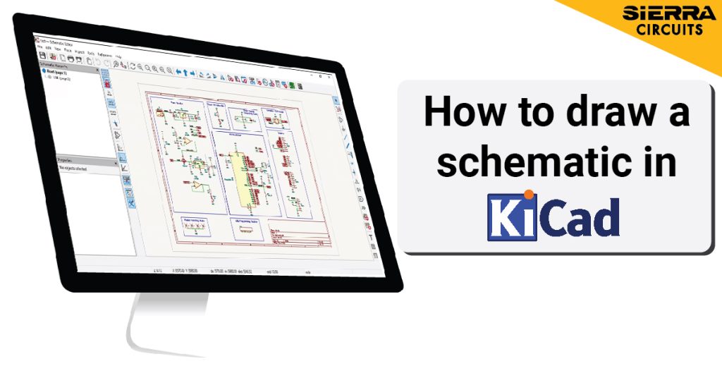
In this KiCad tutorial, you’ll learn how to create a schematic and a symbol library from scratch.
How to create a schematic in KiCad
Creating a PCB schematic is a core part of your design journey. In KiCad, with options to create custom symbol libraries, it helps you easily draw schematics specific to your design.
All the components used in a schematic are described in component libraries. Several libraries provide reasonably simple component management by grouping them by functions or manufacturers.
The component library contains a large variety of preinstalled libraries. The Library Manager menu helps you modify libraries, such as building new libraries by adding and deleting components.
Check out the KiCad library for symbols before creating your own.
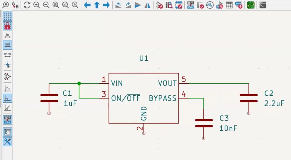
For this tutorial, let us create a power circuitry schematic similar to the image below.

Here, we need to create a new symbol in the component library for the regulator, import capacitors from the KiCad inbuilt library, and provide ground and voltage connections.
In the schematic editor, standard components like capacitors and resistors can be found in the KiCad internal library.
However, if certain component symbols like regulators ICs are unavailable, you can create them using their part numbers.
For step-by-step guidelines on designing a PCB using KiCad, download our eBook.

KiCad Design Guide
10 Chapters - 161 Pages - 180 Minute ReadWhat's Inside:
- Creating a component symbol library
- Setting up board parameters and rules
- How to route differential pairs
- How to place of components
Download Now
Step 1: Add a new project in the schematic editor
To create a new project in the KiCad software, click the File option in the top left corner.
Select New Project, provide a project name, and save it in a folder of your choice.

The side panel now displays a new project. Click on the schematic file to open the schematic editor.
Step 2: Create a new symbol library
To create a new symbol, you need the component package information, which will be present in the datasheet.
We are considering a power regulator IC from Texas Instruments with the part number LP2985-33DBVR for this demo.
The package type is SOT-23, and the drawing is DBV package. This IC has 5 pins, as shown in the below image. The pin configurations are:
- Pin 1- Voltage input
- Pin 2- Ground
- Pin 3- ON/OFF
- Pin 4- Bypass
- Pin 5- Output voltage

It is important to note that a datasheet can have multiple packages, so ensure you search for the correct package using the part number.
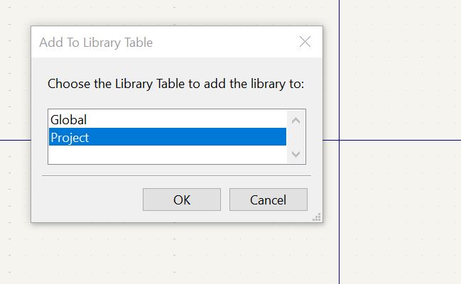
To create a new symbol for this IC, select the schematic symbol editor option (on the editor screen) and click on New Library.

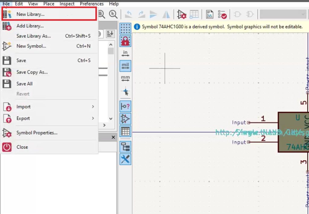
You now have two options: Global or Project. If you are using this library specifically for your current project, you can select Project. If you choose Global, this library will be added to the predefined libraries already in KiCad. Now, save it in the folder of your choice.
The upcoming KiCad version 9 will introduce a new selection filter to the schematic and symbol editor, offering precise control over the elements selected during the editing process. To learn more, see KiCad version 9: exploring the new features.
Step 3: Include new symbols in the library
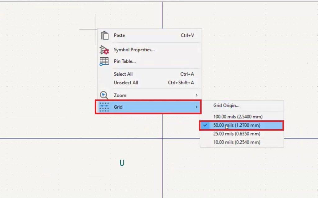
Before creating a symbol, ensure the grid settings are configured. For this, right-click on the screen and select Grid.
Set the value to more than 50 mil for a clear view of the connections.
Next, right-click on the created library and select New Symbol.

Name the symbol and provide a reference designator. For example, ‘R’ for resistors.
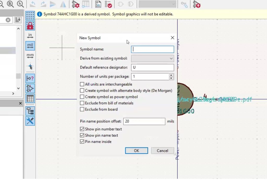
Since we are creating an IC, the default designator will be ‘U.’ Also, add the number of units present in the package.
After entering all the symbol requirements, click OK. Now, you will see the reference designator U on the symbol editor.
To draw the symbol, click the rectangle on the right-hand side and draw a rectangle. This will be the outline of your symbol.

Check out our KiCad plugin for an instant quote from the KiCad editor.

Step 4: Add pins to the new symbol
Click on Add Pin on the right-hand side.

Enter the pin name, number, electrical type (output, input, passive, etc), and graphic style. As we are creating pin 1, we have named it VIN. We have chosen power input as its electrical type.

Place pin 1 on the symbol outline. Similarly, create and add all the remaining 4 pins. Next, hit Save and close the symbol editor.

In the schematic editor, click the Add Symbol option on the right-hand side to place the newly created symbol.
Select the library you have created, choose the symbol, and click OK to place it.
Step 5: Add symbols from the KiCad in-built library
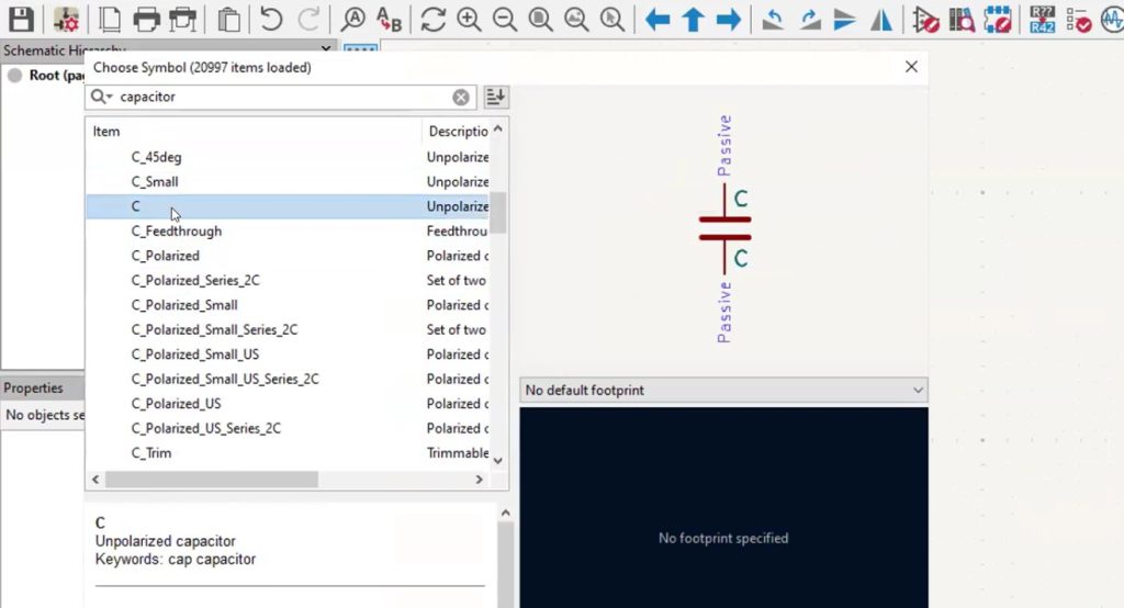
As per the datasheet, we must add decoupling capacitors at VIN, VOUT, and BYPASS pins. We can add the capacitors from the KiCad in-built library.
Click on the Add Symbol and search for capacitors. Select the type of capacitors (polarized, unpolarized, ceramic) you’re looking for, hit OK, and place them on the schematic editor.
Click on the symbol (C for capacitorS) to edit its value.
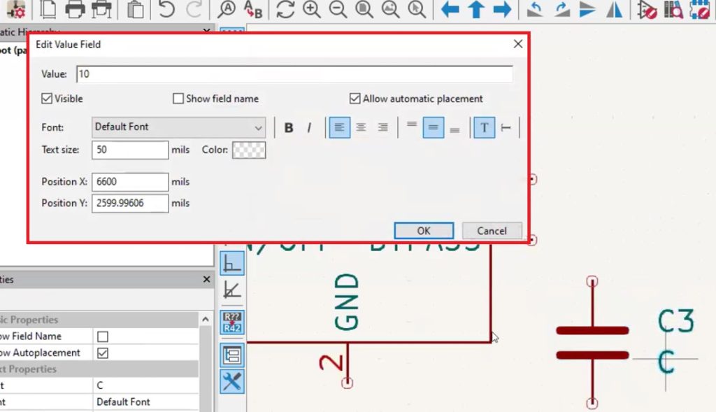
Similarly, you can search for inductors, resistors, and other components required for your design. You can use the copy-and-paste option to place 3 capacitors. Then, edit the capacitance values according to the datasheet.
Step 6: Connect the component symbols
Choose Add Wire to connect the circuit. Here, Pin 3 is an on-off switch. The device will turn on when connected to a high and turn off when connected to the ground.

We will short Vin and pin 3 for this circuit to turn on automatically when the input power is supplied. And connect all the capacitors to their respective pins.
The dot formed in the connection represents the two lines that are connected. If the dot is not present, then the lines are not connected but overlapping.
If needed, you can use the Add Junction option to connect the overlapped line.

Download our eBook for step-by-step guidance on creating custom libraries and linking symbols to footprints in KiCad 9.

KiCad 9 Step-by-Step Guide
6 Chapters - 41 Pages - 30 Minute ReadWhat's Inside:
- A complete KiCad 9 workflow from project creation to production file generation
- Step-by-step guidance on creating custom libraries and linking symbols to footprints
- Practical design checks: ERC and DRC
- Best practices for generating a clean BOM and fabrication-ready Gerber files
Download Now
Step 7: Add power and ground symbols
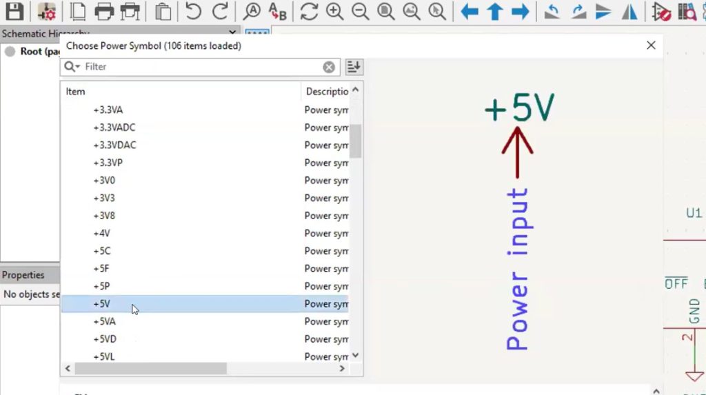
To ground the IC and capacitors, click Add Power. Search for the ground symbol in the pop-up window and add it to the circuit.

Using Add Power, connect VIN to +5V and VOUT to +3.3V.

Step 8: Label the nets
Each net has a name. For example, if you click on the pin 4 net, the connection is named Net-(U1-BYPASS) as default.
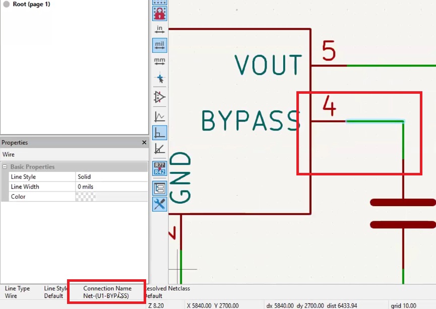
In complex circuits, giving custom names to nets will help identify the connections and their functions.
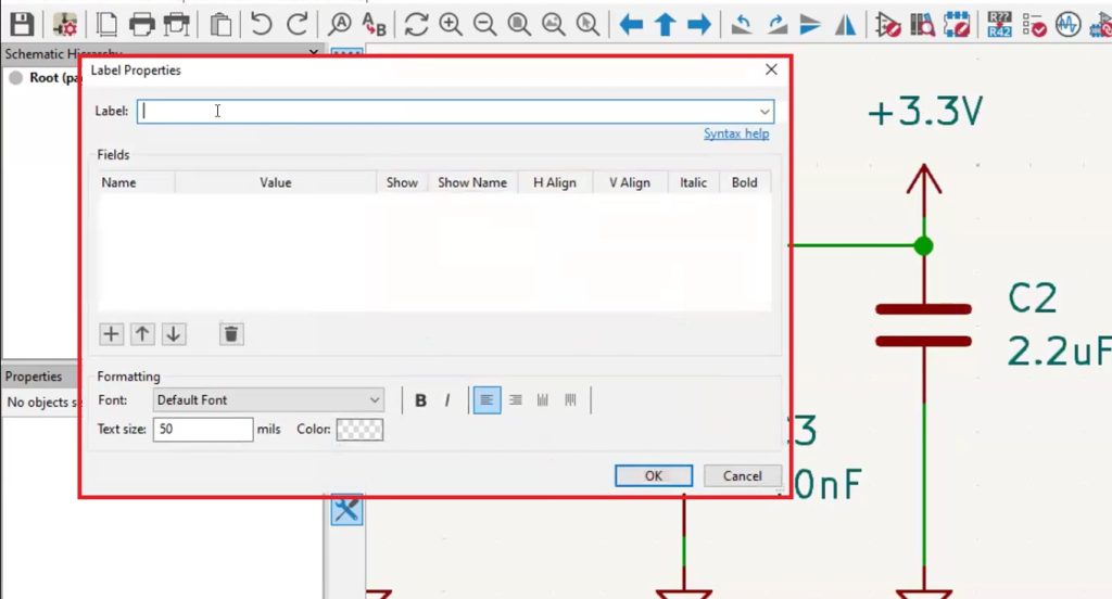
To name a net, select Add Label. In the Label Properties, name it BYPASS and place the label onto the wire.
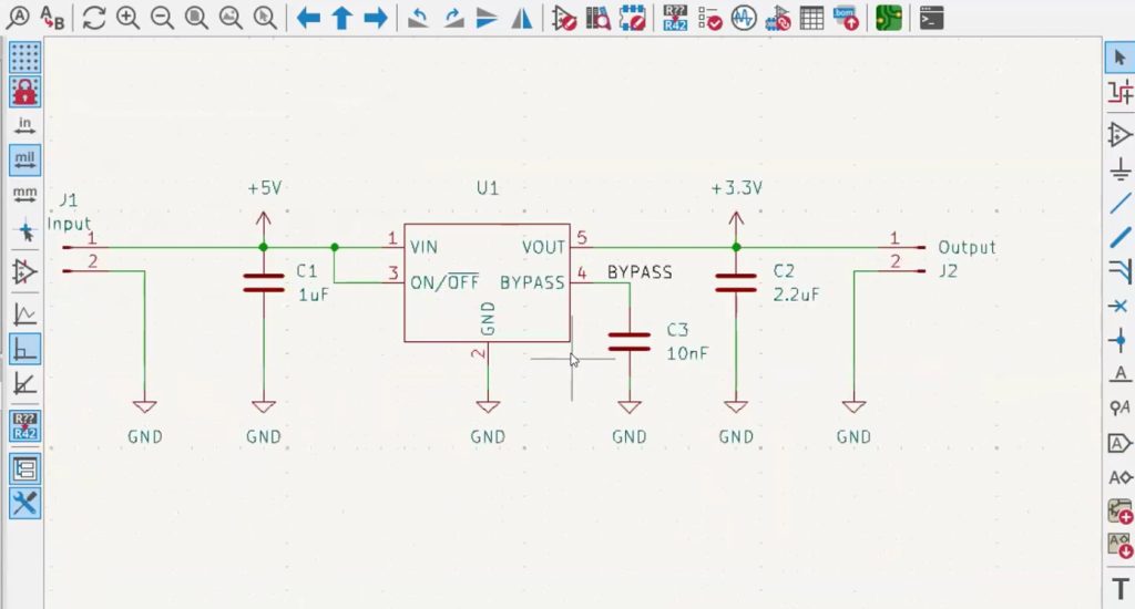
Additionally, you can add connectors from the symbol library to represent the external input and output connections. Make sure you connect the second terminal to the ground. Below is the final schematic of the power supply regulator circuitry.
Need help building a schematic and symbol library in KiCad? Our engineering team can assist you with library setup, symbol creation, and footprint creation to streamline your design process.
You can book a meeting with our experts or call us at +1 (800) 763-7503.

Step 9: Export the BOM file
Before creating the bill of material, configure the properties of each symbol. You can do this using the Symbol Fields Table option present in the top right corner of the schematic editor.

You can add fields like reference designator, value, quantity, DNP, MNP, description, and manufacturer name here. These are a few prominent fields that are essential in a BOM file. You can export the BOM file by clicking the Generate Bill of Materials option.
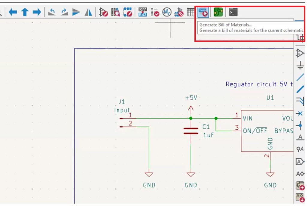
Before exporting, check if the headers and columns have all the required information. Then, choose a folder location to store the bill of materials file. You can also change the file format at this stage.
After configuring the settings, click Export to create a BOM.
Validate your exported bill of material using the BOM checker tool.

Exploring different icon options in the Eeschema
In KiCad’s schematic editor, several main editing options help users create and modify schematics.
Apart from the select, move, rotate, mirror, and delete options, below are the 10 primary editing tools that can come in handy while creating a schematic.
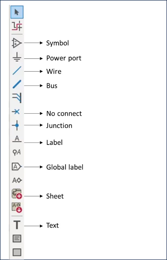
- Symbol: used to add electronic components (symbols) to the schematic. Users can select from a library of symbols representing various electrical components.
- Wire: allows users to draw wires (connections) between components, essential for defining the circuit paths in the schematic.
- Bus: Used to draw a bus, a group of wires that share a common function, such as an address bus or data bus in a digital circuit.
- Power port: adds a power or ground symbol to the schematic. These symbols represent power sources like VCC, GND, or other voltage levels.
- Label: allows users to label wires or nets. Labels are used to identify connections in the schematic.
- Global label: this is similar to regular labels but used for connections that need to be recognized across different sheets in a multi-sheet schematic.
- No Connect: marks a pin on a component as intentionally unconnected. This is useful for avoiding errors during electrical rule checking.
- Junction: Adds a junction point where wires meet. It indicates an electrical connection between intersecting wires.
- Sheet: Using this option, you can create multiple schematic sheets for drawing complex circuits. All the sheets will be aligned in a hierarchically.
- Text: allows users to place text annotations on the schematic. This can be useful for adding notes or instructions.
All these options can also be found under the Place tab at the top left corner of the schematic editor.
Creating custom symbol libraries enables you to tailor your designs specific to your requirements. Whether you are designing simple circuits or intricate multi-sheet projects, KiCad offers an extensive set of features.
Have queries on PCB design, assembly, and manufacturing? Post them on our Forum, SierraConnect; our experts will resolve them.

About Sushmitha V : Sushmitha V has a master's degree in power electronics and has over four years of experience in the PCB industry. Her areas of interest include circuit board manufacturing, assembly, IPC standards, and DFM/DFA practices.


