


Contents
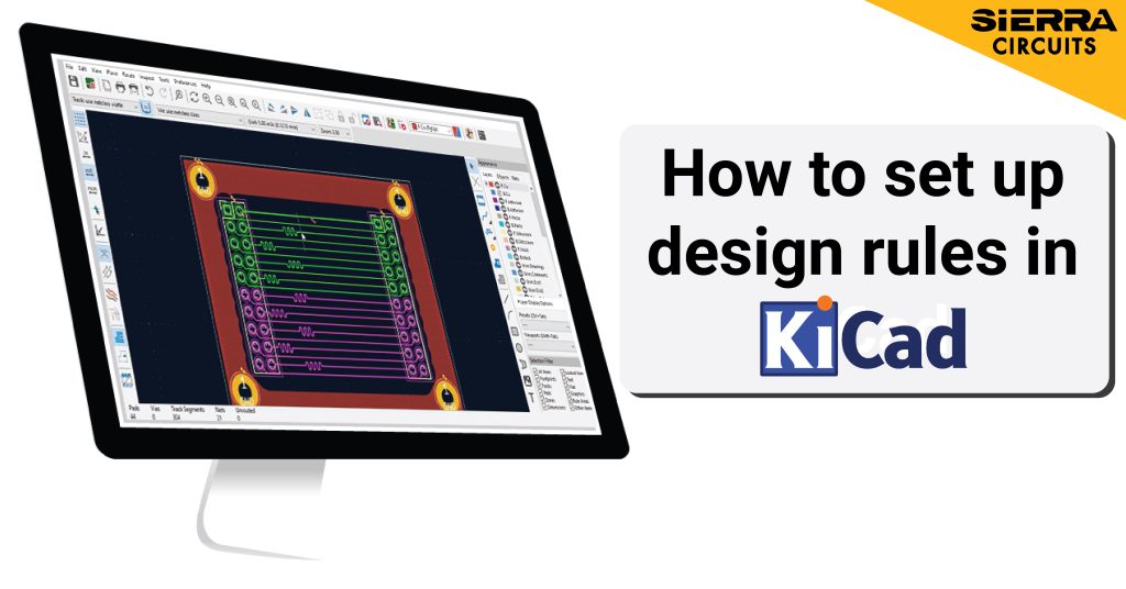
KiCad is one of the best open-source EDA tools, empowering PCB designers with a robust platform for circuit board development.
To get the best out of it, you need to understand how design rules are set in KiCad. These rules include several PCB design elements, such as trace width, clearance, via size, and net classes.
To set up design rules in KiCad, navigate to File > Board Setup > Design Rules.
Highlights:
- Learn how to set constraint values that align with typical PCB manufacturing limits.
- Build reusable libraries of predefined track and via sizes for consistent layouts.
- Use teardrops, length tuning, and net classes to improve reliability and signal integrity.
- Create custom rules and DRC severities that match your specific design requirements.
- Apply design rules efficiently across complex boards using classes and custom conditions.
In this tutorial, you’ll learn the step-by-step procedure for setting up PCB design rules in KiCad.
Watch the full video.
How do you set design rules in KiCad?
Here’s a quick infographic that summarizes the steps for setting the rules.

You can set design rules in KiCad under the Board Setup dialog, where you define clearances, widths, vias, and classes that apply across the layout.
To access the design rules option in KiCad, navigate to File > Board Setup, or use the shortcut on the toolbar. In the Board Setup window, select Design Rules.

Step 1: Set the constraints
Constraints allow you to establish clearance rules such as minimum clearance, track width, and annular width. To access the constraints section, click on Constraints under Design Rules.

The table below shows the typical values for design constraints. Actual values may vary based on your design requirements and the manufacturer’s capabilities:
| Settings | Typical values |
|---|---|
| Minimum clearance (For 1 Oz copper thickness) | 4 mil |
| Minimum track width (For 1 Oz copper thickness) | 4.5 mil |
| Minimum connection width | 5 mil |
| Minimum annular ring | 4 mil |
| Minimum via diameter | 14 mil |
| Copper to hole clearance | 8 mil |
| Minimum through-hole | 6 mil |
| Hole to hole clearance | 8 mil |
| Minimum uVia diameter | 8 mil |
| Minimum uVia Hole | 4 mil |
| Silkscreen min item clearance | 2 mil |
| Silkscreen Min text height | 30 mil |
| Silkscreen min text thickness | 5 mil |
The constraints section is divided into 7 segments, each allowing you to set various parameters. Below are the segments and their corresponding parameters:
- Copper: Minimum clearance, track width, connection width, annular width, via diameter, copper-to-hole clearance, and copper-to-edge clearance
- Holes: Minimum through-hole diameter and hole-to-hole clearance
- Microvias: Minimum microvia diameter (finished) and minimum microvia hole
- Silkscreen: Minimum item clearance, text height, and text thickness
- Arc circle approximated by segments: Maximum allowed error in line segments
- Zone fill strategy: Minimum acceptable number of thermal relief spokes connecting a pad to a zone
- Length tuning: Stack-up height in track length calculations. When utilizing a via during length matching, select this option to automatically consider the via height.
To import settings from an existing board design, click on Import Settings from Another Board and select the design file. Next, choose the settings you want to import and click on Import Settings.

To learn more, download the KiCad Design Guide.

KiCad Design Guide
10 Chapters - 161 Pages - 180 Minute ReadWhat's Inside:
- Creating a component symbol library
- Setting up board parameters and rules
- How to route differential pairs
- How to place of components
Download Now
Step 2: Specify the custom dimensions for traces and vias
In the Pre-defined Sizes section, you can establish a library of pre-defined tracks and vias. This feature is essential for maintaining consistency and ensuring that frequently used sizes are readily available. This reduces the manual input each time you create a new track or via.

To add a new track, via, or a differential pair, click on the + button.

Step 3: Add teardrops for tracks and pads
Teardrops significantly enhance PCBs’ reliability by reinforcing the connection between pads, traces, and vias. They act as stress relievers, reducing the risk of cracking and trace detachment due to mechanical stress or thermal expansion.
KiCad allows for a custom teardrop design for circular and rectangular pads, as well as between tracks themselves, providing flexibility in PCB design.

In this section, you can set the following characteristics of teardrops:
- Best length (L): The ideal teardrop length. It’s based on the width of the connected pad or trace.
- Maximum length: Maximum allowed teardrop length.
- Best width (W): The ideal teardrop width based on the size of the connected component or trace.
- Maximum width: Maximum allowed teardrop width.
- Maximum track width: The teardrops are only generated when the connected track is narrower than a specified percentage of the pad width.
- Prefer zone connection: If enabled, a teardrop won’t be created if both the pad and the track are already connected to a zone (like a ground or power plane)
- Edges: These radio buttons specify whether the teardrop edges need to be straight lines or curved.
- Curve points: Number of points in a curve; more points make the curve smoother.
- Allow teardrops to span 2 track segments: If selected, the teardrop extends into a second track segment if the first segment is too short for a full teardrop.
You can also add teardrops to existing connections quickly. To do this, go to Edit and click on Edit teardrops.

A dialog box appears with the following sections:
Scope: Here, you can define the types of objects affected, such as PTH pads, SMD pads, vias, or track-to-track connections.
Filter items: This allows filtering by criteria like net, net class, and layer. You can also apply filters based on round pads, pre-existing teardrops, or selected objects.
Action: You can remove or add teardrops based on your size and shape requirements. If a teardrop already exists, it will update with the new settings.
To add teardrops for individual vias and pads, double-click the pad or right-click on the pad and select Pad Properties.
A dialog appears as shown below.

Now, go to Connections and enter the dimensions as per your requirements.
Also, read how to autoroute a PCB layout in KiCad using the FreeRouting plugin.
Step 4: Perform length tuning for traces
In the Length-tuning Patterns section, you can tune the length of single tracks and differential pairs by adding serpentines to your traces. This is one of the new updates in KiCad.

This section 3 segments:
- Single-track length tuning: Adds serpentine shapes to increase the length of a single track to the target value.
- Differential pair length tuning: Similar to single-track tuning, it adds serpentine shapes to a differential pair to adjust the length of both tracks in a differential pair to meet the target value.
- Differential pair skew tuning: Adds length to the shorter track in a differential pair to eliminate skew (phase difference) between the positive and negative sides.
When setting up tuning patterns, you need to adjust the following parameters:
- Maximum/minimum amplitude (A): Set the maximum and minimum amplitude for the tuning pattern.
- Spacing(s): Specify the spacing between meanders.
- Corner style: Choose between filleted (rounded) or chamfered corners.
- Radius(r): Enter the serpentine’s radius as a percentage of the spacing and amplitude.
- Single-sided pattern: Configure the tuning pattern to be single-sided, restricting it to one side of the baseline instead of the default style that positions meanders on both sides.
Need help setting up design rules in KiCad? Our engineering team can assist you with setting up DRC configuration, clearance rules, and trace width constraints to ensure your design meets industry standards.
You can book a meeting with our experts or call us at +1 (800) 763-7503.

Step 5: Group the nets using net classes
In the net classes section, you can create a hierarchical structure library for organizing multiple nets. Grouping the nets within a net class ensures uniform application of design rules to the entire group.
Every net in KiCad is assigned to a specific net class. If a net is not added to a specific class, it will automatically be included in the default class. To add a new net class, you click on the + button and enter the following details:
- Name of the net class
- Clearance
- Track width
- Via size
- Via hole
- Microvia size
- Microvia hole
- Differential pair width
- Differential gap

Here, we have created net classes with the names Group1, Group2, and POWER.
We have a plugin that enables you to get a PCB quote directly from the KiCad design tool. Download the KiCad plugin now to get an instant price estimation.
Step 6: Define the custom rules
The infographic below shows the steps to create custom rules.

This segment allows you to set custom design rules for your design.

Here’s a template to define a custom rule:
(version <number>)
(rule rule_name> <rule_cause>…)
(constraint <constraint_type>…)
(condition “<expression>”
(layer “<layer name>”)
(severity <severity_name>)
Version: Here, you just have to enter a number. The rules will be assessed based on the version. The latest version number will be considered for DRC.
Rule name: Choose a descriptive name for your rule that accurately reflects its purpose. Enclose this name within quotation marks. (rule <rule_name> <rule_clause>…)
Constraint: This clause defines the actions to be taken when the rule is triggered. You can include multiple constraint clauses to impose various constraints, such as clearance and track width, on objects that meet the same conditions.
Condition: It specifies which objects the rule applies to. It uses expressions to detail the conditions.
Layer: This defines the board layers to which the rule applies. You can use specific layer names or shortcuts like outer (for front and back copper layers) and inner (for internal copper layers). If no layer is specified, the rule applies to all layers.
Severity: Define the severity level for a rule violation. This defines how violations should be handled—whether as errors, warnings, exclusions, or ignored
Let’s look at an example from the syntax help dialog in KiCad. This rule sets a minimum clearance between vias of different nets.
(
rule “Distance between Vias of different Nets”
(constraint hole_to_hole (min 0.254 mm))
(condition “A.Type == ‘Via’ && B.Type == ‘Via’ && A.Net != B.Net”)
)
In this example,
- Rule name: “Distance between Vias of different Nets”
- Constraint: Minimum hole-to-hole clearance of 0.254 mm (10 mils)
- Condition: Applies to vias (A and B) that belong to different nets
By following this structure, you can create and customize rules to ensure your PCB design meets all necessary requirements. Be sure to consult the syntax help dialog for precise instructions and thoroughly test your custom rules to ensure they function as intended
For more, download the KiCad 9 Step-by-Step Guide.

KiCad 9 Step-by-Step Guide
6 Chapters - 41 Pages - 30 Minute ReadWhat's Inside:
- A complete KiCad 9 workflow from project creation to production file generation
- Step-by-step guidance on creating custom libraries and linking symbols to footprints
- Practical design checks: ERC and DRC
- Best practices for generating a clean BOM and fabrication-ready Gerber files
Download Now
Step 7: Assign violation severity
The Violation Severity segment lets you assign the level of DRC violation when the rule is not followed.

You can set the severity for electrical, design for manufacturing, and schematic parity segments using the radio buttons. After providing your input, click OK.
KiCad is a versatile tool for electronic circuit design and corresponding PCB design, which requires familiarity and expertise. This guide on setting up KiCad for your PCB design will help you design faster and better.
Are you having trouble with your KiCad PCB design? Our design experts can answer your questions on our PCB forum, SierraConnect.


