


Contents
PCB constraint settings are necessary for a successful board design. Modern applications demand high-speed, high-density, complex stack-up design. It is tough to find and fix every single fault in a circuit board.
To help designers, multiple PCB design tools have come up with various constraint management settings. You can set the default parameters, fix different rules for a net or net class, or specify constraints to fulfill the requirements. The constraints include the trace width, minimum trace clearance, differential lines settings of trace and space, component and trace gap from the edge of the board, etc.
The constraint settings management seems to have a negative undertone. But in PCB design, it is considered to be the backbone of a design. The main objective is to manufacture a proper, functional board that satisfies the design requirement rightly. In this article, we will focus on the implications of constraint management settings in Altium Designer and Allegro PCB Editor.
Significance of constraint settings
A constraint region is an area on a layer of a board in which a specific net follows some particular rules. Outside the constraint region, that net does not obey the same rules. To demonstrate the whole thing, consider a signal net with a line width of 8 mils. If you pass that net over a BGA with a 0.8 mm pitch and an air gap of 15.5 mils between two pads, the remaining clearance on the two sides of the pad will be around 7.5 mils. Each side will have a gap of 3.75 mils which is less than the recommended standard of 5 mils. Hence, you have to reduce the line width to 5 mil and the remaining space on both sides will be 5.25 mil.
How to create a constraint region in Altium Designer
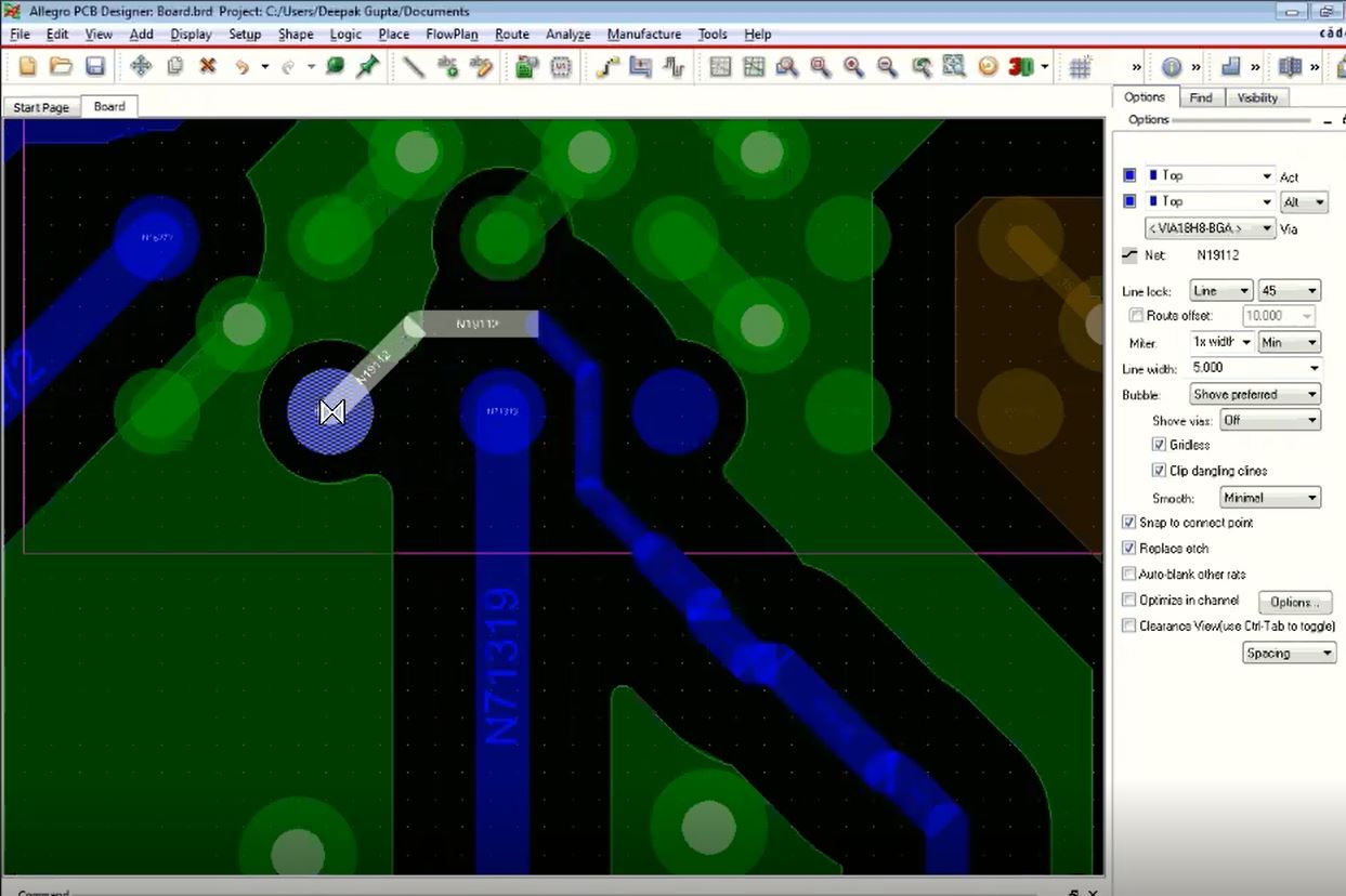
How to create a constraint region in Allegro
The constraint settings management helps you to avoid manufacturing errors and ensures the high-quality electrical functionality of the board. Here, we will briefly discuss some vital manufacturing and electrical aspects that need effective constraint management to avoid circuit board errors.
Electrical factors for constraint settings
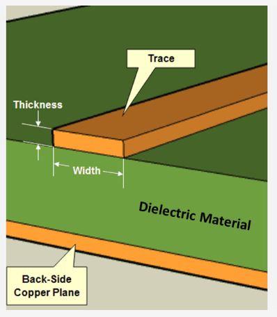
Trace width
Trace width is a critical factor in PCB layout and design for carrying high currents. If the current goes beyond the specified carrying capacity, the trace could heat up and burn out. To prevent this, it must be mentioned in the constraint rules that wider traces are needed to carry high-current.
Impedance matching
In PCB design, traces are not only considered as a connecting medium to pass signals but also act as a transmission line. Impedance greatly impacts how signals propagate through the board, and how power is transmitted between components. Accurate impedance matching for a signal trace is required to have maximum performance. Trace dimensions should be set to achieve the required impedance to ensure signal integrity.
The constraint management for routing high-speed signals, especially above 100 MHz is vital. To achieve proper transmission of a high-speed signal, you can follow these constraints settings:
- Controlled impedance is required along the electrically long lines to prevent back-and-forth reflection. You can define a tolerance limit for impedance mismatching among source, transmission line, and load.

- Trace spacing and width should be mentioned to meet the impedance matching requirements.
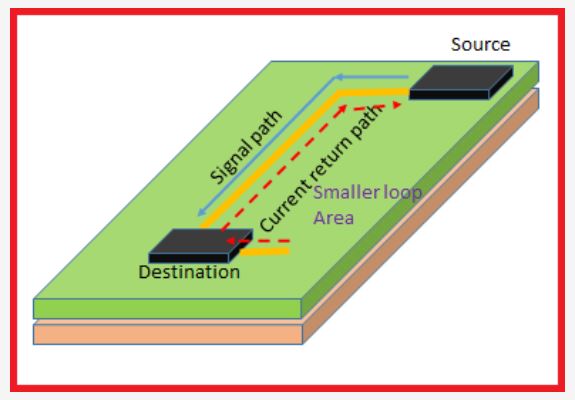
- The return path is responsible for the overall loop inductance of a circuit. The allowable deviation of the target impedance is the determining factor of the allowed return path deviation.
Propagation time matching
Traces are used to route the clock, address, and data signals. These are designed with suitable timing synchronization with others to function efficiently. Constraint settings for trace length matching and propagation time matching for such signals become necessary to function correctly.
Signal integrity
Signal integrity is the most concerning factor in PCB design. To avert disruption, basic routing protocols are defined.
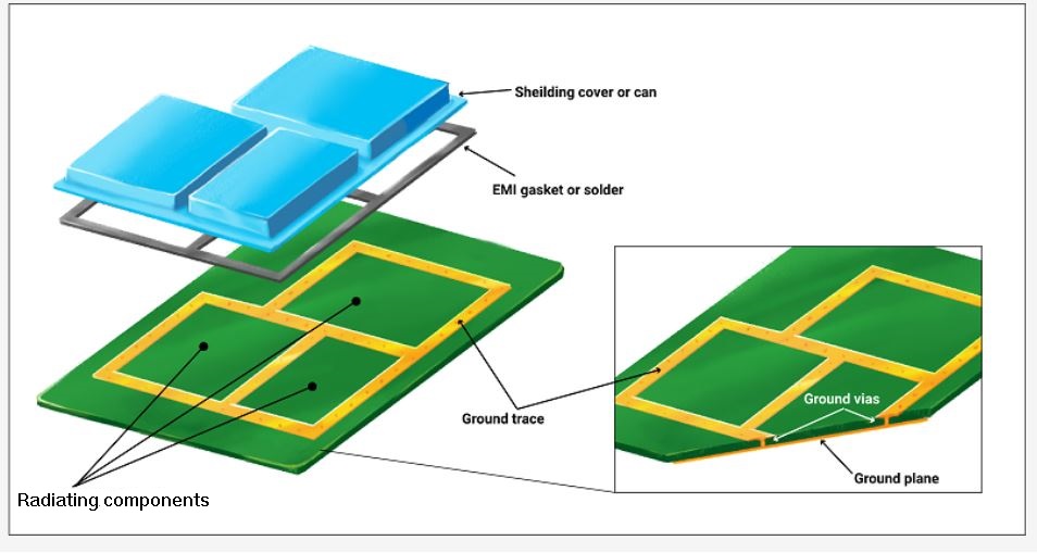
- Electro-magnetic interference (EMI): Often, some traces emit radiation on the board. Incidentally, the radiation can cause disturbance to the circuit itself or the neighboring devices. To guard the source trace against radiating and the victim by the effects of EMI, traces are needed to be routed between ground planes to introduce shielding. Proper matching of impedance reduces the signal ringing and thus removes EMI.
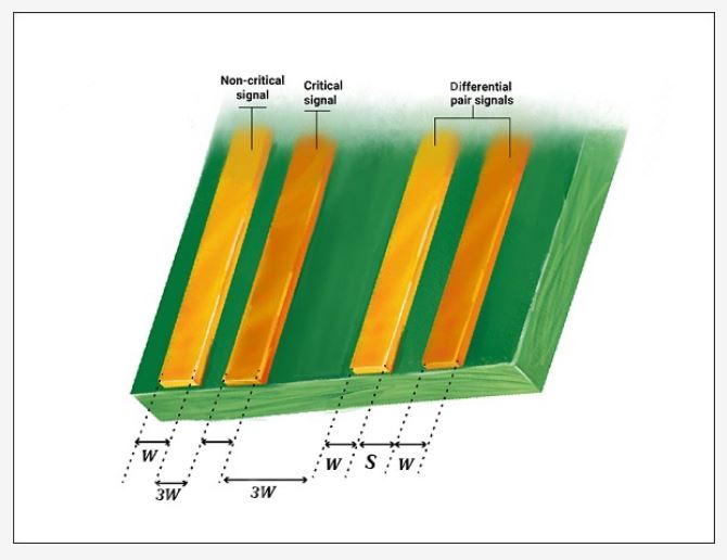
- Crosstalk: This is associated with trace dimensions and geometry. Sometimes spacing between two traces is not sufficient, so interference of signals occurs subsequently. Normally, 3W spacing between unrelated signals is recommended to avoid crosstalk where W is the trace width.
- Reflections: Reflection is cross-linked to impedance mismatching and termination.
- Transient ringing: In-circuit board design or electronic system, ringing refers to sudden oscillation in output voltage or current like a ripple. It occurs because of random input switching and impedance mismatching.

Signal Integrity eBook
6 Chapters - 53 Pages - 60 Minute ReadWhat's Inside:
- Impedance discontinuities
- Crosstalk
- Reflections, ringing, overshoot and undershoot
- Via stubs
Download Now
Managing assembly issues with constraint settings
Assembly
The components in a board have to be organized appropriately for a smooth automatic component installation. Spacing between the components needs to be set to ensure manufacturability and assembly of the board without shorts. For large and non-standard components manual installation is required that demands enough room.
Accessibility
Designing a PCB involves the arrangement of various components, traces, connectors, and switches. It is crucial to make them accessible by technicians for both automatic and manual testing.

Solderability
Improper soldering causes intermittent shorting and thermal imbalances in the circuit. To avert these, relevant component arrangements and sufficient space availability are needed in automated soldering systems.
Various PCB constraints and design rules
How to set up design rules in Altium Designer
How to set up design rules in Allegro
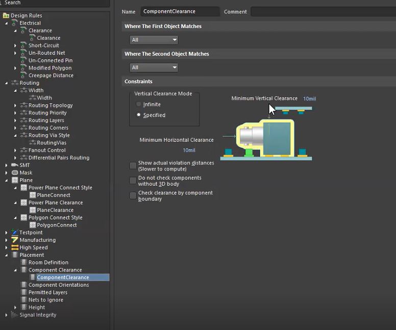
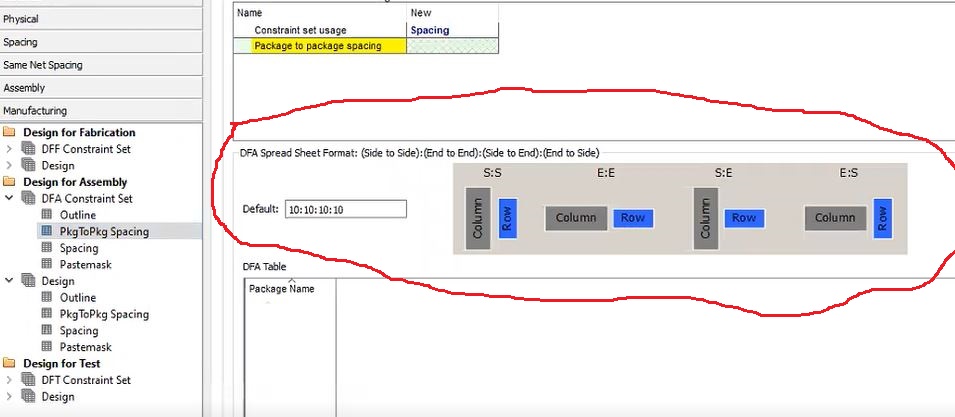
Component clearance in Altium Designer and Allegro
You can arrange the component clearance with other parts of the board with constraint management. The specific region of placement of any particular component or the region prohibited for individual components can also be controlled.
Altium Designer
Go to Rules under Design → PCB Rules and Constraints Editor→from the left sidebar choose Placement → select Component Clearance → set vertical and horizontal clearance according to the design specifications.
Allegro
Go to Set up → under Constraints select Constraint Manager → select Design for Assembly → open Pkg to Pkg Spacing → you can adjust the spacing of the components from side to side and end to side.
You can book a meeting with our experts or call us at +1 (800) 763-7503.

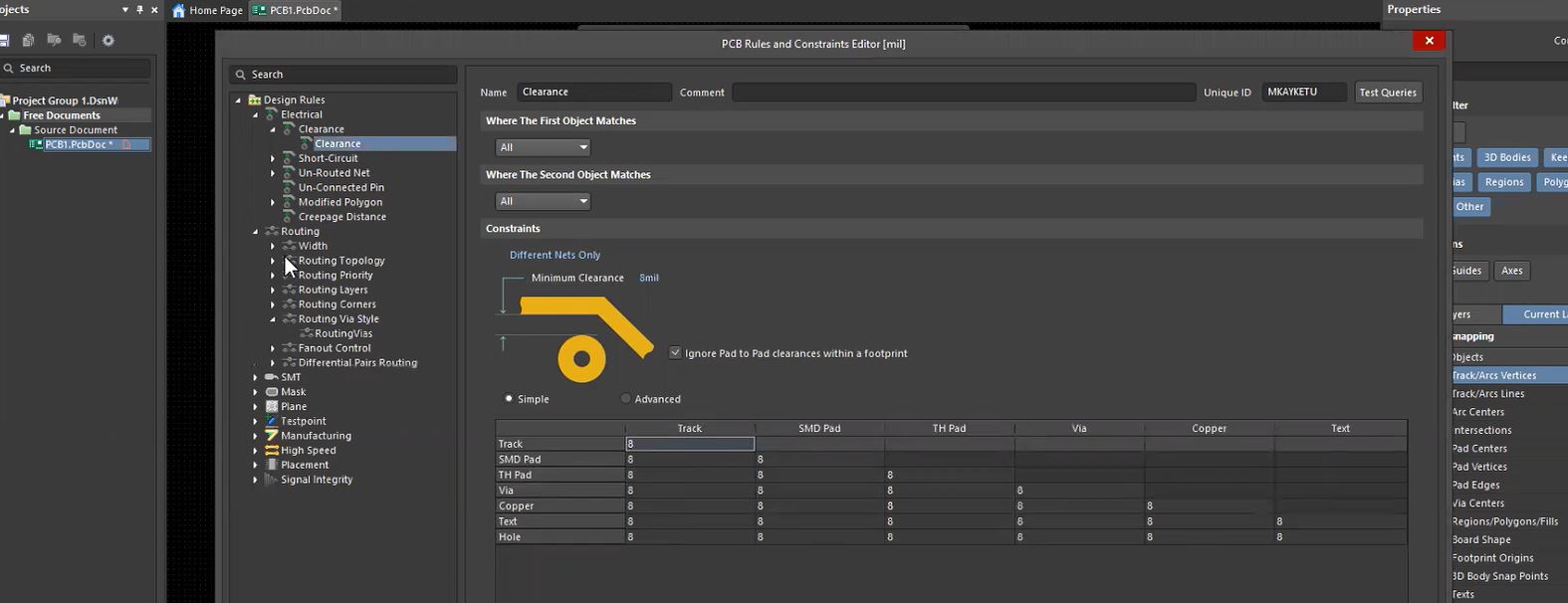
Electrical object spacing in Altium Designer and Allegro
Designers can control the spacing between a trace to pad, trace to via, trace to trace, trace to other metal objects, drill holes, and board edges. Additionally, particular layer clearance can be mentioned as per design requirements. Check manufacturing tolerances.
Altium Designer
Go to Rules under Design → PCB Rules and Constraints Editor→ from the left sidebar choose Electrical → click Clearance → adjust the clearance between two different electrical objects.
You have options to select the mode, simple or advanced as per your requirement.
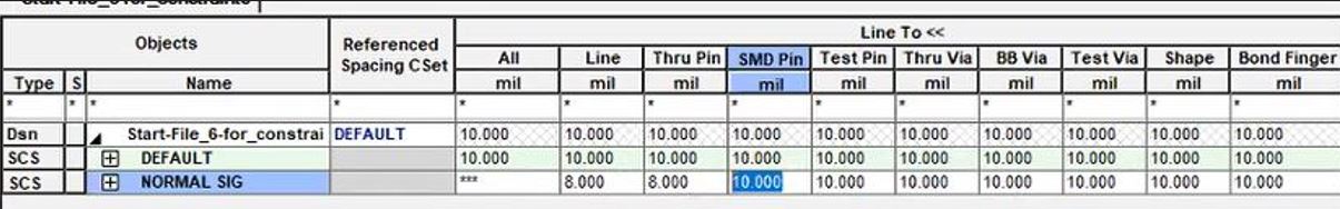
Allegro
Open Constraint Manager → go to Spacing present on the left menu→ select All Layers under Spacing Constraint Set → create a Spacing Cset → set the spacings between one object to another.

Trace width for routing signals
Trace routing is one of the critical factors in constraint settings. This consists of maximum and minimum trace width, and length matching with other traces. Trace width can also be set up for a particular net or a net class, controlled impedance traces, differential pairs, or other specific traces like clock signals.
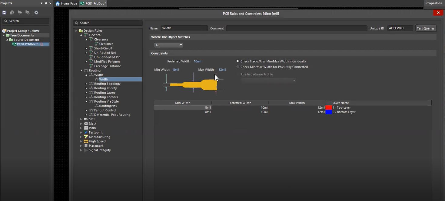
Altium Designer
In the PCB Rules and Constraints Editor window, select Routing from the left menu → set maximum, minimum, and preferred width according to your design.
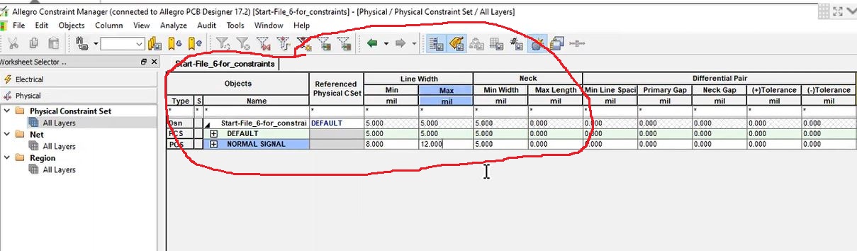
Allegro
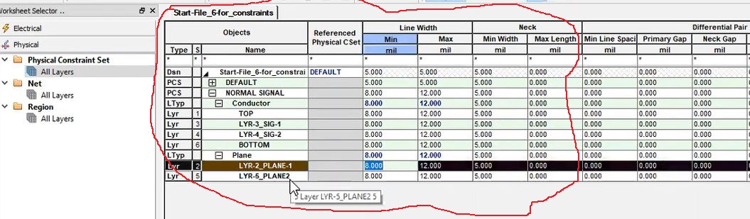
Open Constraint Manager → go to Physical Constraint Set → create a Physical Cset → adjust maximum and minimum line width.
To expedite the component placement and routing process in Allegro and Altium Designer, see Auto-grouping of repetitive PCB design blocks
Power plane settings in Altium Designer and Allegro
Designers can have an overview of how the traces and vias will be connected to the power with thermal stability from constraints. The pattern and allowable width can be specified too.
Altium Designer
Connection style of power plane: Go to Plane from the left menu → click Power Plane Connect Style → Plane Connect → select among Direct Connect, Relief Connect, or No Connect.
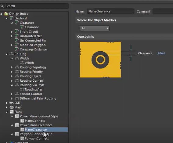
Power plane clearance: Go to Plane Clearance from Power Plane Clearance → adjust the clearance.
Connection style of the polygon: Select Polygon Connect Style from Plane → Polygonconnect → choose among Direct Connect, Relief Connect, or No Connect.
Allegro
Go to Set up → open Cross-section → check the design stack-up.
This stack-up can be seen in Physical Constraint Set under Constraint Manager.
Vias constraint management in Altium Designer and Allegro
You can describe the types of vias, via clearance to components on the circuit with constraint management. Layer stack-up can also be depicted in the case of blind or buried via and microvia.
Altium Designer
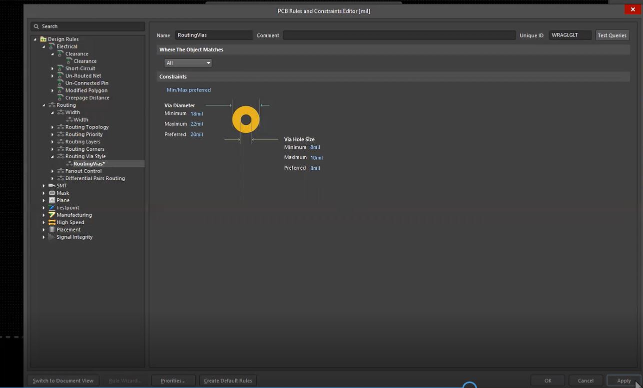
Select Routing Via Style from the left sidebar → go to Routing Vias → set up the rules for via hole size and via diameter → click Apply.
Allegro
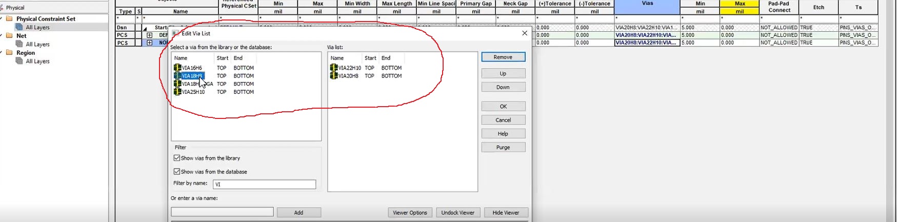
Open Constraint Manager → select your set under Physical Constraint Set → choose the vias from the library and preset database as per the design specifications.
To know how castellated pins are designed, see how to design a castellated circuit board using Altium Designer and Allegro.
Altium Designer or Allegro?
PCB designers take help from constraint management tools to achieve a precise design. Depending on efficacy, trustability, and user accessibility you can use Altium Designer or Cadence’s Allegro constraint methods. Here, we are going to compare these two tools.
Constraint region customization
The constraint region is a sub-class where you can define the specific spacing and physical rule.
In Altium Designer, you have to create a room object and place it on the board. Subsequently, you can set the specific rules for that region particularly.
In Allegro, you have to set the customized rule area from the constraint region box. After this, this region can be added to a constraint set for future use.
User interface
Irrelevant and not-so-attractive user interfaces always matter while choosing the right option for PCB designers. Both in Altium Designer and Allegro, the color panels are quite charming.
Altium Designer: The graphical representation of component physical spacing is great. The matrix which includes various component sizes and spacing is also beneficial in designing a board.
Allegro: The spacing choice is a little bit complicated. As there is a lack of proper guidance in selecting physical spacing by using graphics in the constraint set itself.
Convenience and accessibility
This section is based on two factors- convenience in using the constraint manager and applying the rules appropriately.
Altium Designer: Creating rules is easy but the application of these requires a proper draft to prioritize the constraints.
Allegro: Rule creation may be a tough choice without the right training or guidance. Though, once you get to know, implementation is just a piece of cake.
Efficacy and trust
In Altium Designer, rule creation is easy with the help of graphics and images. But the design of a high-speed circuit requires code generation to set up differential pairs, net class, and some constraints. The priorities are fixed accordingly. Sometimes overlapping or unwanted issues may hamper the reliability here.
In Allegro, we can see that the constraint management system includes large spreadsheets. You can set up your constraints as per the design requirement. These constraint sets are added to a particular net or group. Moreover, manually any constraint can be altered for a specific object. There is a very rare chance of having any error in the created design.
Does ‘Help’ really help?
In Altium, you can have great context on a specific feature or tool and examples are there to show you the right direction. But if you don’t know the exact term, researching the topic and getting to know about that is a difficult job.
You can get profound knowledge from Allegro documentation. As soon as you open the window against a particular feature, you can learn about the terms related to that feature very easily.
Both the Altium Designer and Allegro design tools aid to create a high-performance board with minimum design cycles. Based on the design parameters, requirements, and your expertise you can pick the suitable tool. If you are interested to learn about controlled impedance design then you can download our design guide.

Controlled Impedance Design Guide
6 Chapters - 56 Pages - 60 Minute ReadWhat's Inside:
- Understanding why controlled impedance is necessary
- Stack-up design guidelines
- How to design for impedance
- Common mistakes to avoid
Download Now
About Poulomi Ghosh : Poulomi is a microwave engineer specializing in EMI, EMC, RF, and high-speed electronics. As a senior technical writer at Sierra Circuits, she creates advanced engineering articles and webinars for hardware engineers and PCB designers.


