High-density interconnect (HDI) PCBs involve a higher wiring density per unit area compared to conventional circuit boards. To achieve this high density, designers have to consider the right via technologies, built-up laminations, and high-signal performance. Let us have a look at these requirements for an HDI design.
What is an HDI PCB design?
HDI boards are compact designs with smaller vias, pads, and traces. This technology enables a lower layer count. Thus one HDI board can perform the same function as any conventional board but with a smaller form factor.
Designing high-density boards require early planning. Switching over to an HDI after realizing the application’s space constraints during the manufacturing process will be a tiresome task in terms of redesign, time, and money. Hence, as a designer, first analyze and recognize the design needs before you start designing. To master the HDI design, see how to master HDI PCB design.
Standards for high-density interconnect boards
Stick to the below-mentioned standards while designing HDI designs:
- IPC/JPCA-2315: High-density interconnect structures and microvias design guide.
- IPC-2226: Standard specifications for material characterization, microvia formation, interconnecting structures, and selection of design rules.
- IPC/JPCA-4104: This standard establishes the qualification and performance specifications for the dielectric materials to be used for high-density interconnect structures.
- IPC-6016: General specifications for the high-density substrate.

HDI PCB Design Guide
5 Chapters - 52 Pages - 60 Minute ReadWhat's Inside:
- Planning your stack-up and microvia structure
- Choosing the right materials
- Signal integrity and controlled impedance in HDI
- Manufacturing considerations for higher yields
Download Now
HDI specification
Boards with the specifications given below can be considered HDI designs:
- The lines and spaces should be ≤100 μm
- Vias with a diameter ≤150 μm
- Capture pads ≤400 μm
- Capture pad density of >20 pads/centimeter2
Material selection for HDI
The next step is the selection of the right material for HDI manufacturability that meets the temperature and electrical requirements. The chosen material will affect the electrical performance of the traces. The dielectric loss of the material also makes an impact. Other parameters such as maximum withstanding temperature, the maximum frequency of signals, and CTE are equally important during material selection.
Some of the popular materials used for HDI boards are:
- Normal speed and loss: FR4 family
- Medium speed and medium loss: Nelco N7000-2 HT
- High speed and low loss: Isola I-Speed
- Very high speed, very low loss (RF/microwave): Isola Tachyon 100G
- Once the material is finalized, plan an efficient PCB stack-up and microvia structures.
Different high-density interconnect stack-ups
There are two basic HDI standard structures called sequential laminations/build-up and every layer interconnect (ELIC). Out of these two, sequential lamination structures are most commonly used. In this structure, at first, cores are constructed and laminated. Afterward, drilling, plating, and filling are carried out. This layer is then laminated along with other layers and again the drilling, plating, and filling processes are repeated.
ELIC is used in applications with high interconnectivity requirements. In this structure, all the microvia layers can be freely interconnected.
The number of laminations is one of the most important factors while designing an HDI board. This decision is based on the type of stack-up used in the board design.
The standard high-density interconnect stack-ups are as follows:
a) 0-N-0 stack-up
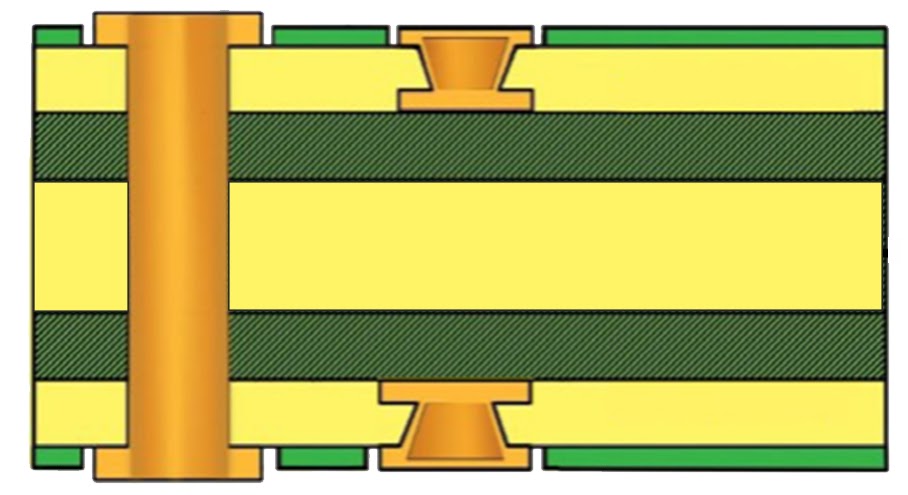
This stack-up is built using a single lamination. N represents the number of layers of base/core/first laminations. 0 shows the number of sequential lamination steps added. With the increase in the complexity of the stack-up, the required steps will increase. Hence, cost increases as well.
b) 1-N-1 stack-up
Here, 1 represents one sequential lamination on either side of the core. This adds two copper layers for N+2 layers.
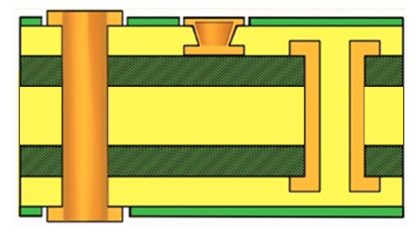
c) 2-N-2 stack-up
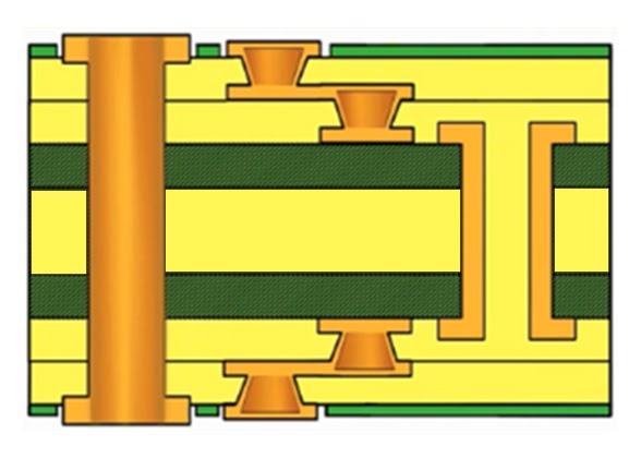
Similar to the stack-up shown above, 2-N-2 has 2 sequential laminations. 2 sequential laminations will add 4 copper layers and the total becomes N+4 layers. Both of these stack-ups do not have stacked microvias, which are explained at a later stage.
These are just some examples of the standard stack-ups used in HDI technology. The designs of the build-ups can vary depending on the requirements of the board. The number of sequential laminations can be increased as per demand, but keep in mind with the increase in the number of laminations, the cost and time for manufacture also increase.
Via technologies used in HDI
Different types of PCB vias are employed while designing and manufacturing HDI boards. To achieve the desired wiring density, controlled depth vias are implemented in the HDI design. Let us have a look at the different via technologies used in HDI.
Microvias for HDI PCBs
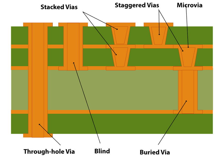
Microvias are laser-drilled vias that have a diameter typically less than 150µm. The plating of copper inside these small vias is a difficult task. Because of this reason, microvias are usually not more than two layers deep.
Microvias are further classified based on their arrangements as shown below:
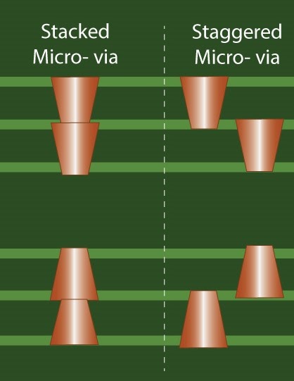
- Stacked vias:
These are microvias present in different layers that are piled on top of one another. These vias require copper filling. - Staggered vias:
Staggered vias are drilled in different layers and are scattered in position. They do not require copper filling. Hence requires fewer process steps. For more details, see design and manufacture of staggered and stacked vias in PCBs. - Skip vias:
Skip vias skip one layer in between with no electrical contact with that layer. This layer will not form an electrical connection with the via.
The via design depends on the individual design constraints of an HDI design. Using microvias reduces the layer count and helps in the BGA breakout.
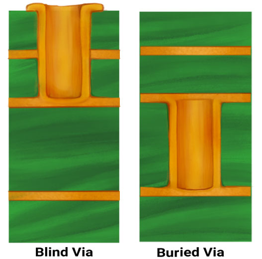
Blind and buried vias are also involved in this type of design.
The best choice out of these vias is made depending on the chosen stack-up type and the type of components installed.
Aspect ratio (AR) of laser drills
The aspect ratio of laser-drilled microvias is an important parameter. The AR for a microvia is defined as the ratio between the drill depth and the diameter of the drilled hole.
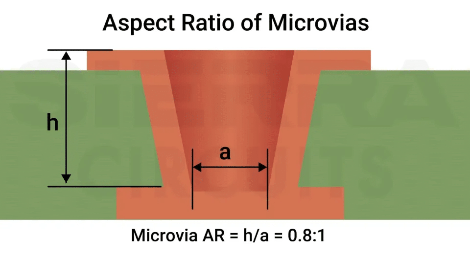
When the aspect ratio is higher, the process of copper plating inside the vias becomes non-uniform and inadequate.
The aspect ratio of microvias is defined to be less than 1. The current standard value is 0.8:1. For a dielectric of 3 mil, the hole diameter will be 3/0.8 = 3.75 mil. This implies that the microvia diameter should be larger than the height of the next layer that it penetrates.
These are the main aspects involved in the design of HDI circuit boards. Right from selecting the material, to deciding the type of vias and stack-ups, play a crucial role in achieving the desired functionality. That is why much effort goes into the proper design of these parameters.
See our FAQ on HDI PCBs.


