


Contents
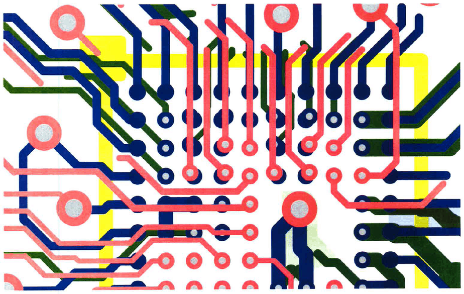
One thing PCB designers will all agree on is that to breakout a BGA, you need precision and discipline. When you breakout a BGA, you basically apply a fanout solution. You route traces from those fanouts to the perimeter of the device prior to general routing of the PCB. Here are two examples of a .4mm BGA breakout.
Watch us perform a .4mm BGA breakout in Allegro
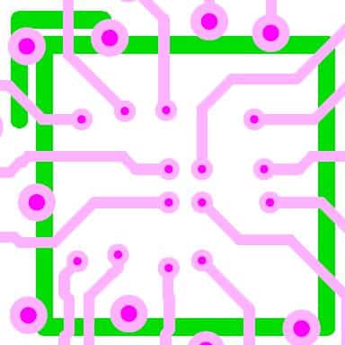
.4mm BGA breakout
Becoming a PCB master for HDI starts with learning how to breakout a BGA. BGAs have the highest density of I/O connections and array pins on a device, which is the most complex part of the layout.
Since there is not just one but multiple ways to breakout a BGA, we are giving you an example of how to breakout a .4mm BGA. A good design practice is to do the layout part by part. You need to make sure that you will be able to fan out and connect all the pads under the BGA. Another good design practice is to draw short tracks.
When planning out how to breakout (or route) a .4mm BGA, the overall size and the pinout of the part need to be thought through. This way, you can use the most cost-efficient technology. It is not just about the fact that the pads are .4mm apart and figuring out what the widths and gaps are that work.
When fanning out a .4mm BGA, the geometry does not work out so that you can route a trace between the pins. The traces and gaps are just too small to go down enough layers to get all the pins fanned out.
So with a .4mm BGA, blind and buried vias are required. The pins on the outside row in the BGA are routed on Layer 1. The pins on the next row in the BGA are routed on Layer 2. And so on. The way the BGA is pinned out will determine how to route the BGA.
In the configuration above, the problem is: What can you do with the GND pin? Drilling from Layer 2 to Layer 3 will cost more.
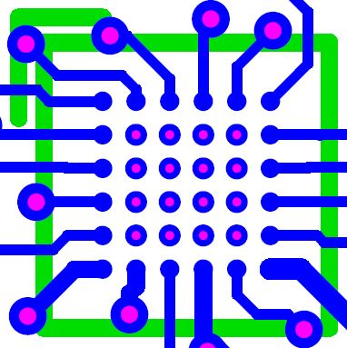
How to breakout a .4mm BGA: Example #1
This part is a standard .4mm BGA. The best way to fan it out is to use blind and buried vias and a multi-lamination fabrication.
Start off by adding a Layer 1 to Layer 2 blind via on all of the GND pins of the BGA. (This is a hole in the BGA pad that will tie that pin to the GND plane on Layer 2.) Now you are done with all of the GND pins and do not need to follow the routing described below.

HDI PCB Design Guide
5 Chapters - 52 Pages - 60 Minute ReadWhat's Inside:
- Planning your stack-up and microvia structure
- Choosing the right materials
- Signal integrity and controlled impedance in HDI
- Manufacturing considerations for higher yields
Download Now
The routing plan
Route the outside row or ring of pins (24 pins, row 1 and 7, and A and G) on the top side of the board, Layer 1. You may need to route out some of the GND pins on the outside row. And not just add a 1 to 2 via in the BGA pad.
Add a Layer 1 to Layer 2 blind via to the next ring of pins (16 pins, row 2 and 6 and B and F). Then route this ring out on board Layer 2. Layer 2 is a GND plane, so these Layer 2 routes can only route out a short distance. Then you add a standard top to bottom via. Do not cut off the GND plane with these short Layer 2 routes, such that the GND plane is cut up and the pins are not connected.
Then, on the next ring of pins (8 pins, row 3 and 5, and C and E), add a Layer 1 to Layer 2 blind via. Now, add a Layer 2 to Layer 3 via. And route these nets out on board Layer 3.
The BGA pin in the very center of the chip will need to be worked out on Layer 2 or 3. To learn the techniques we used to breakout the inner pins of 0.4 mm BGA, read our case study on routing microcontroller and BGA in rigid-flex PCBs.
Learn How To Breakout a .5mm BGA
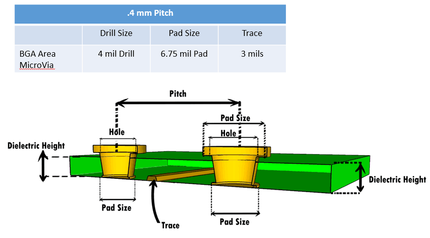
Pad and drill sizes for .4mm BGA
There will be no traces between pads on the top layer. Therefore, the pads can be 10 mils and have a 5.7 gap between them. For the larger pad, let the manufacturer drill a 4 to 6-mil laser drill for the buried and blind vias. The distance between the board layers will determine the best drill size so they can plate the hole shut and make a flat pad for the BGA, etc.
Sequential lamination
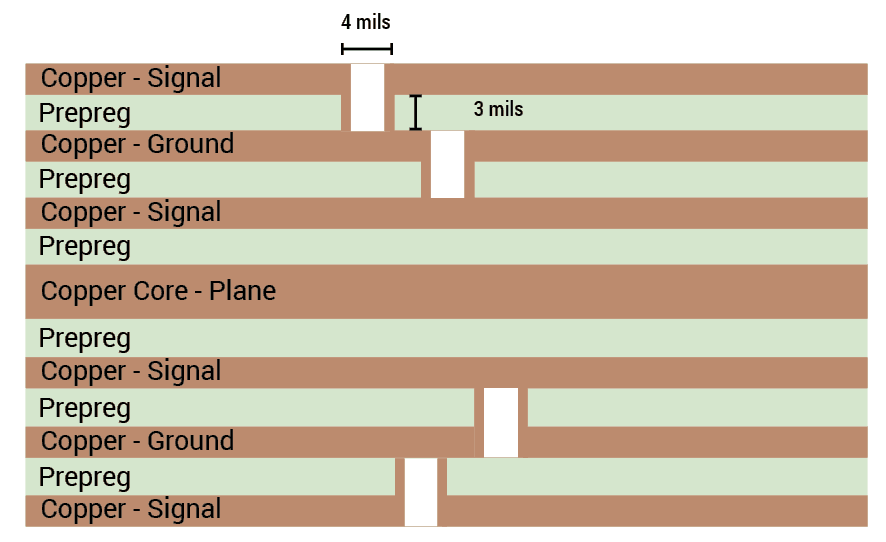
Let’s pretend that this is an 8-layer board.
Board Layers 2 through 7 will be laminated together. Then, you can laser drill from Layer 2 down to Layer 3. This is your 2 to 3 buried via. Note that you can use a Layer 7 to 6 buried via as well. Same for Layer 2 to 7. But the 2 to 7 needs to have a bigger drill and pad.
Board Layers 1 and 8 will now be laminated to the board. A laser drill will be done from Layer 1 down to Layer 2 (Layer 10 to 9 if needed).
Then, the standard through via is drilled top to bottom – here again, a bigger drill and pad are required.
In your Gerber files, you have parts placed around the .4mm BGA. The fanning out and adding standard-size vias and trace width and spacing will take up a lot of room around the BGA.
Need help breaking out BGAs? Our engineering team can assist you with fanout strategies, via placement, and trace routing to ensure successful BGA escape routing.
You can book a meeting with our experts or call us at +1 (800) 763-7503.

How to breakout a .4mm BGA: Example #2
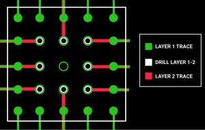
This is a .4mm BGA pitch on a 6×6 matrix. It has 4-5 mil trace/space, with 4-mil lasers and 8-mil pads. The routing strategy includes stacked and staggered vias.
This PCB has 4-mil vias. The material thickness between layers 1 – 2 should be 4 mils, max. The aspect ratio rule requires 4 mils of dielectric between layers 1 and 2. Stackups must be kept symmetrical, so there must also be 4 mils of dielectric between layers 7 – 8.

Layer one: signal
For outer layers like layer 1 of the BGA breakout, the outermost pins can simply be fanned out. There is no need to worry about routing between pads. The outer layer pad size is determined by the chip’s footprint. Pad size depends on BGA ball size. Pad size does not need to be the same size as the balls. Solderballs are always smaller than pads.
Layer two: ground
This stackup shows layer two with layer one pads. The pads have been offset. There is mostly short routing because it is a ground plane. Short stub fan-out is used throughout the BGA. We don’t want to “cut up” the ground on layer two. Longer routing will be found on layer three. The BGA is connected to ground on layer 7. Other areas outside the BGA are connected to layer two.
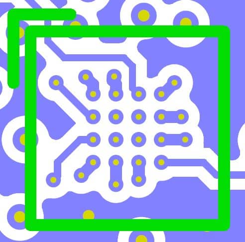
Layer three: signal
The third BGA row was routed on layer three. The four middle pins could not have been routed before. The second BGA row was completely routed on layer three as well: it had been fanned out on layer two and has now been completely routed out.
Key takeaways:
- A large majority of the .4mm routed pitch BGAs require an HDI PCB.
- If your IC designer leaves enough space, the best location for a mechanical through via is within the center of the BGA.
- To meet BGA requirements, it is okay to break other PCB design rules. Within tight BGAs, all bets are off.
- Tie the signal to the ground outside densely populated areas.
- For better power feed, tie to ground planes using through vias. Return paths run more smoothly when closer to signal layers. Return paths are also crucial for high-speed signals.
- Copper layer thickness defines trace/space.
- Route less on ground planes to keep their integrity—don’t cut up the ground planes.
- Pad size, BGAs, and routing on outer layers are determined by chip size and pitch.
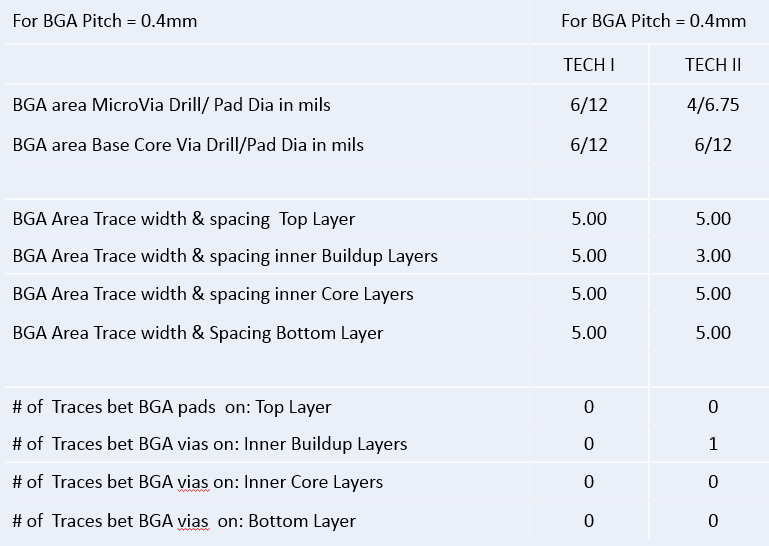
Technology level for .4mm BGA
Robert Feranec’s fanout strategy
Robert Feranec, the founder of FEDEVEL Academy, explained, “Be careful about drawing the connections all at once. It is a good design practice to do the layout part by part. If you have a BGA, the first goal is to get out of the BGA. Be sure that you can go out with all the pads and all the pins under the BGA. Do not fully route all the interfaces. But instead, just route a little bit of track. Then stop routing to place vias. Or draw the tracks for different parts just a little bit out of the BGA area. Make sure that you will be able to fan out and connect all the pads under the BGA. You can then start connecting all the interfaces.”
He further added, “If you only draw short tracks, it is very easy to delete them and redo parts of the layout under the BGA. Because you did not fully route the tracks. So you can just delete them and try to find a way to fan out all the pins. This practice is much easier. It will save you a lot of time since you only have to deal with a small part of your layout. You want to avoid finding yourself in a difficult position once you have fully routed your BGA and you need to take out only one pin, for example. If that happened, you would have to deal with a lot of tracks just to be able to remove one signal.”
Robert concluded, saying, “There are some exceptions, like memories or high-speed interfaces. In this case, you can fully route the connections between the BGA and the memories or the high-speed interfaces before you finish the fanout of all the pads.”

High-Speed PCB Design Guide
8 Chapters - 115 Pages - 150 Minute ReadWhat's Inside:
- Explanations of signal integrity issues
- Understanding transmission lines and controlled impedance
- Selection process of high-speed PCB materials
- High-speed layout guidelines
Download Now


Watch our demo here: How to Fanout a 0.4 mm Pitch BGA