Contents
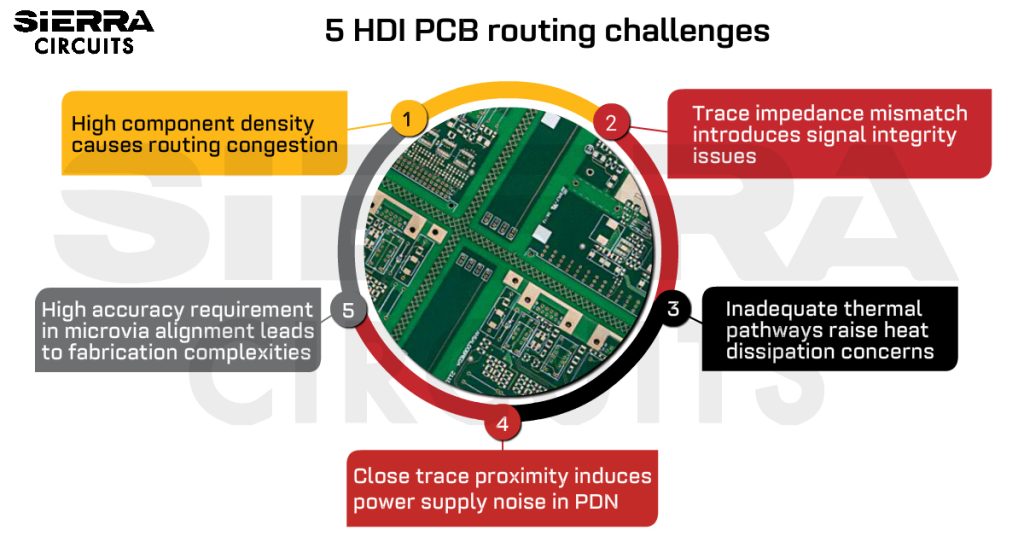
High-density interconnect (HDI) represents the cutting edge of the printed circuit board industry today, due to the demand for signal integrity and compact circuit boards. But do you master HDI board design like you should?
In our previous article series becoming a PCB design master, we have focused on designing for circuit board assembly and achieving faster time to market. This article will hone in on the finer points designers must know in order to master HDI boards.
What is high-density interconnect (HDI) PCB?
HDI boards feature higher wiring density per unit surface area than standard boards. HDI use some or all the below features that reduce the size of the board:
- Lines and spaces less than or equal to 100 micrometers.
- Vias less than or equal to 150 micrometers.
- Capture pads less than or equal to 400 micrometers.
- Capture pad density of more than 20 pads per centimeter square.
The increased interconnection density allows for enhanced signal strength and improved reliability. Additionally, thanks to design efficiency and space maximization, HDI boards make it possible to manufacture smaller, more powerful electronic devices.
Why HDI circuit board?
Why is there even a separate category of board technology called HDI? Well, when the lines get smaller than 65 microns (2.559 mils), the ability to etch your trace and space is diminished. You can’t really use a traditional etching process. For example, typical etching on a standard board allows for a very thick resist along with standard imaging on an LDI machine and you essentially have plenty of space for any tolerances needed to etch those spaces. In a microelectronic environment, you don’t have any of those leeways. The features are so close together that traditional etching processes don’t work.
HDI technology is the best choice for board designers when they require a higher density of components. So what makes HDI different from the standard board? Mainly three things:
- Microvias replacing through-holes in higher component density areas of the circuit board
- Layer stack-up alternatives to accommodate microvias
- Arranging vias to improve routing
#1 Microvias replacing through-hole vias – Why microvias for HDI?
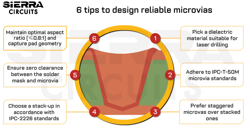
HDI uses microvias instead of through-hole vias where higher precision is required. Laser drilled microvias can be used up to a drill hole depth of approx 100µm. Since microvias have a short barrel they do not face problems with different CTE (coefficient of thermal expansion) values of substrate and copper. That’s why microvias are more suitable than through-hole vias.
The best practice for designing an efficient HDI is to replace the most common vias (blind, buried, or through-holes) with microvias. Move the most commonly used layers (Ex: GND or PWR) to the top of the stack-up if they don’t have components and traces on them (GND and PWR planes need to be solid and unbroken). This stack-up arrangement can either eliminate the vias required or allow to replace the through-holes with microvias. As the microvias don’t go throughout the thickness of the board, this provides more space on the other layers. Hence, this practice can improve the routing density of the inner layer and reduce the number of signal layers.
#2 Layer stack-up alternatives to eliminate through-hole vias
Different stack-up arrangements are used in the HDI structure to reduce the number of through-holes and the number of inner layers. The ground and power planes are the most used layers to drill vias. HDI PCB designers can reduce the number of stack-ups by placing these layers at the top of the stack-up, say layers 2 and 3. The top and bottom layers are normally used for component placement.
Thin dielectric layers less than 0.005 inches are used to separate GND and PWR planes. This provides a low power supply impedance and also enables the use of ‘skip vias’ from layer 1 to layer 3.

#3 Arranging vias to improve routing
Proper arrangement of vias is crucial in HDI board designing. The arrangements aim at providing better signal integrity and improving routing space in the inner layers. Here’s a depiction of stacked vias:
Stacked vias
Fine-pitch BGAs create a necessary complication with HDI where the design rules are chosen to not provide clearance for staggered blind vias. The stacking of two microvias or placing a microvia on top of the buried via is needed when this situation arises.
Boulevards created by via placement
Blind vias are arranged to form a boulevard structure. Boulevard formation can reduce the total number of power layers and doubles up the routing space.
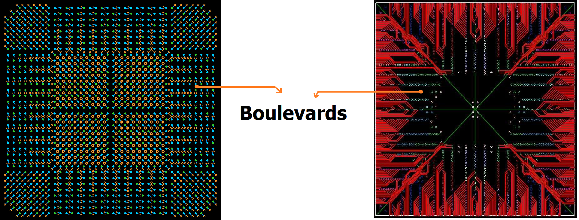
These structures can be created by skip vias, multiple buildup, or sequentially laminated, and laminated vias. It is also used for routing of high-speed critical nets using only the cross-over from horizontal to the vertical connection of small and low inductance blind vias.
Also read: The history of high density interconnect
HDI PCB designing
In the past, high-density interconnect has run up against the wall of board technology. And today, with lots of innovation and investments, we are able to push the boundaries of circuit board fabrication when it comes to trace widths and spaces. So HDI PCB design is essentially defined by the spaces between traces as well as all copper features. In that regard, we want to define HDI and microelectronics and provide a few suggestions to you on understanding design rules and how they interplay with each other to get a good design.
For a thorough understanding of HDI architecture, we are obligated to provide you the information on the basics. First, we’ll check out possible stack-up structures and then discuss how to approach the manufacturer with the design idea.
What are the IPC standards an HDI designer must know?
Before we discuss HDI designing and design rules in detail, we would like you to get accustomed to the standards that govern HDI PCB design.
IPC/JPCA-2315: Design guide for high-density interconnect structures and micro vias.
IPC-2226: Standard specifications for material characterization, microvia formation, interconnecting structure, and selection of design rules.
IPC/JPCA-4104: This standard helps in identifying the material required for the HDI structure. Qualification and performance specification for dielectric materials for high-density interconnect structures.
IPC-6016: Contains general specifications for the high-density substrate. Qualification and performance specification for HDI structures.
Also read: Happy Holden Discusses HDI
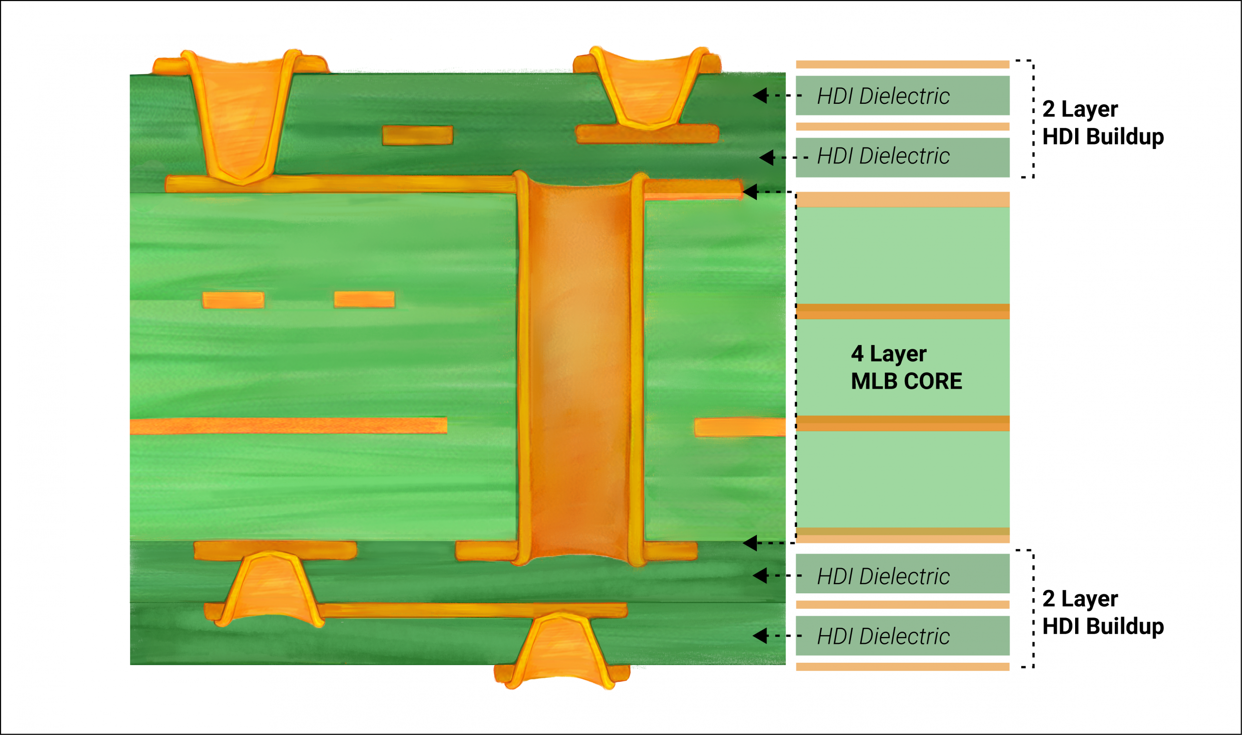
Basic HDI structures
Let’s look at the basic structures of HDI PCB technology before discussing the design rules and the other aspects. The two basic HDI structures that exist are the “buildup”/ “sequential lamination” and the “any-layer” structures.
The build-up structure is the most commonly used type of HDI structure. The sequential lamination process is used to build this structure. Cores are constructed and laminated first, then drilling, plating, and filling in this plane is done. After this process, this layer is laminated with other layers, and the drilling, plating, and filling processes repeat.
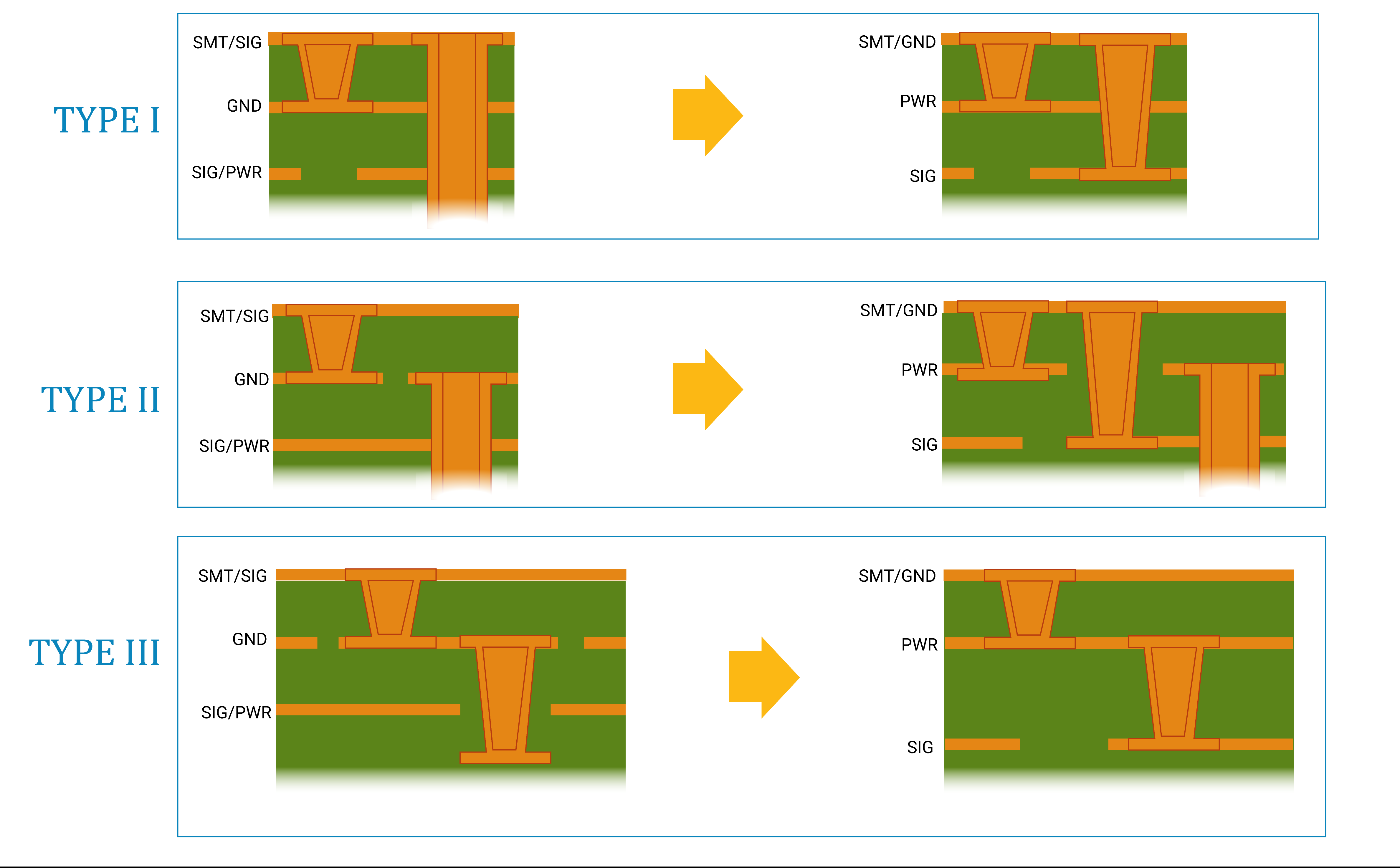
According to IPC 2226 standard, HDI structures are classified into six types:
- Type I 1(C) 0 or 1(C) 1: Construction with both plated microvias and plated through-holes used for interconnection. Type I construction allows only a single microvia layer on either single side or both sides of the core. This is represented here as 1(C) 0 and 1(C) 1. Here, 0, 1, …n represents the number of microvia layers on either side of the core, and (C) represents the core.
- Type II 1(C) 0 or 1(C) 1: Type 2 allows the through-hole vias to be placed in the core before the HDI layers are applied and may have through-hole vias connecting the outer layers from surface to surface. In the case of microvia layers, it is similar to type I.
- Type III 2>=(C)>=0: Two or more HDI layers added on the top of the core with through-hole vias or from the surface to surface through-vias are allowed.
- Type IV >=1(P)>=0 : P is a passive substrate with no electrical connecting functions. Here, microvias are used as a redistribution layer over an existing drilled and plated passive substrate.
- Type V coreless: Coreless constructions using layer pairs.
- Type VI constructions: “Any-layer” construction, alternate for coreless construction using layer pairs.
Let us check the basic structures of sequentially laminated HDIs.
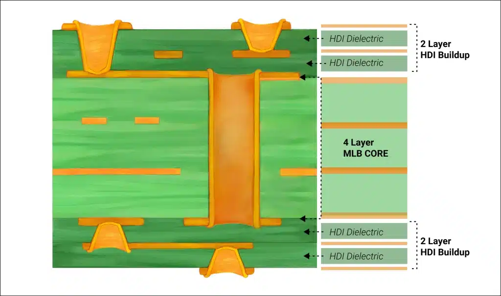
In the 1+N+1 type of stack-up, ‘1’ represents one sequential lamination on either side of the core. One sequential lamination adds two copper layers for a total of N+2 layers. There is one extra lamination on the top layer and stacking of the vias is allowed. This buildup is suitable for BGA with lower I/O counts and its mounting stability is excellent.
Now, check the 2+N+2 stack-up shown above. This buildup contains 2 layers of high-density interconnection, suitable for BGA with smaller ball pitch and higher I/O counts. These designs use copper-filled staggered or stacked micro vias that are commonly used in high-level signal transmission applications.
The “Any-layer” structure is another approach used in HDI PCB design. Any-layer boards are the next-level advancement in HDI that follows the type VI HDI standard. Any-layer technique is used for high-level interconnection applications because all of the microvia layers can be freely interconnected.
In this method, microvia layers are used as redistribution layers in the prepreg or we can say they are floating in prepregs. Microvia in a layer is constructed first, following the process of drilling, filling, plating, printing, etching, and lamination. Then, other layers are stacked above the existing layer following the same process.
The number one question designers usually ask is… what pad sizes, what hole sizes and how tight can the traces and spaces be together? These are good questions as long as you’re designing a relatively standard board. You can’t just look at our HDI PCB manufacturing capabilities page and not understand how they interact with each other. For standard products, it may work, but as you get into more complicated boards such as HDI or microelectronics with finer feature sets, it may not work.
To learn more about pad design, read What is a Pad in PCB Design and Development?
HDI layer construction example
Let’s say you’re doing an HDI construction with very fine lines and you are going to do, let’s say a 2+4+2 type of stack-up. So 2+4+2 essentially means you’re going to have a buried sub-construction which we will mechanically drill and plate. Now, if we have to do fine lines on layer 3 of the buried sub-construction, that becomes problematic. The processes on layer 3, don’t allow for fine line technology. Whereas on layer 2, you have more leeway for your fine lines.
Now when you get into that feature set, designing the whole board with those feature sizes is not the same as designing just a small portion of the board with those feature sets. If you can loosen up the spacing with bigger pad sizes and bigger drill sizes in non-dense areas it will make it easier for the manufacturer and less costly for you… especially if you’re going into production.
So we really wanted to dive deep on that distinction. Even though our capabilities would say 35 microns is the minimum trace and space, it is not a feature size that we would recommend or be able to manufacture across the entire design.
“Increased interconnection density allows enhanced signal strength.”
Becoming an HDI master
Higher density means HDI designers must constantly keep layout and spacing in mind, among other factors. The following are four tips on avoiding common HDI board design mistakes.
1. Make space a priority
Considering space during HDI PCB design means more than squeezing in as many components as possible. First, designers must ensure boards can be properly maintained in the future. Determining the amount of space between specific components and opting for an extra room is a requirement. This can also make things simpler during board manufacturing. Via diameter, pad diameter, and trace width should all be taken into account before implementation begins. Otherwise, circuit boards may have to be completely redesigned, requiring further time, money, and energy. Read our case study on designing 8 and 14-layer HDI PCBs with stacked vias to learn the techniques we implemented to build reliable stacked microvias.

Design for Manufacturing Handbook
11 Chapters - 96 Pages - 90 Minute ReadWhat's Inside:
- Annular rings: avoid drill breakouts
- Vias: optimize your design
- Trace width and space: follow the best practices
- Solder mask and silkscreen: get the must-knows
Download Now
2. Understand the implications of blind and buried vias
HDI boards incorporate blind and buried vias to make the most of limited space. Blind vias connect outer layers to inner layers but do not go through the entire board. Buried vias connect multiple inner layers but do not go through outer layers. While practical and functional, blind and buried vias differ from traditional through holes and greatly influence the overall design of boards. Designers must focus on the vias as they not only affect the construction of boards but also impact signal performance based on their location and placement.
3. Avoiding solder-related issues
If designers aren’t careful, solder can cause multiple issues. For instance, via-in-pads may siphon solder away from specific components, leading to shoddy connections. One workaround to this issue is avoiding the use of via-in-pads. Unfortunately, depending on the board design and its applications, sometimes this is impossible. In such cases, covering via-in-pads with a solder mask can eliminate the issue. However, using a solder mask can lead to its own complications. Solder masks with large openings can allow substantial amounts of solder to reach the board, resulting in tombstoning or disconnected pins. It’s vital for designers to monitor potential solder issues before designing begins.
Refer to our post on 8 common errors in SMT to learn more about various soldering defects such as tombstoning, cold solder joint, etc.
4. Incorporate design reviews
This applies to all circuit board design projects, yet deserves special focus within HDI. It can be difficult for designers to step away from their own work and spot small errors. This becomes doubly hard when designers are working with an even higher density of components. Incorporating advice and perspective from other designers, technicians, and more is a strategic way to fix small mistakes before they become larger, more costly problems. It can be tempting to skip design reviews to meet tight deadlines, but ultimately, such reviews are the ideal way to save time and money.
Also read, HDI PCB case study: partner early for HDI board design to learn how early collaboration streamlines HDI PCB development, reduces risks, and ensures high-quality results.

Design considerations for HDI PCB design
HDI boards require certain design considerations to be taken into account during the designing process. Let’s refer to each of them:
Smart component selection
Usually, an HDI board contains SMD (high pin count) and BGA (≤ 0.65 mm) components. The spacing/pitch between their pins should be chosen wisely since it helps to define trace widths, via type, and board stack-up.
Use of microvias
Use microvia or sequential build-up technology (< 0.15 mm diameter). It can help you to achieve twice the number of pins/area than through-hole pins. These microvias are used to form the escape area of dense components (high I/O, micro BGA). The low inductance of microvia makes them suitable for high-speed applications, for connecting power planes with a decoupling capacitor, and where noise reduction is required.
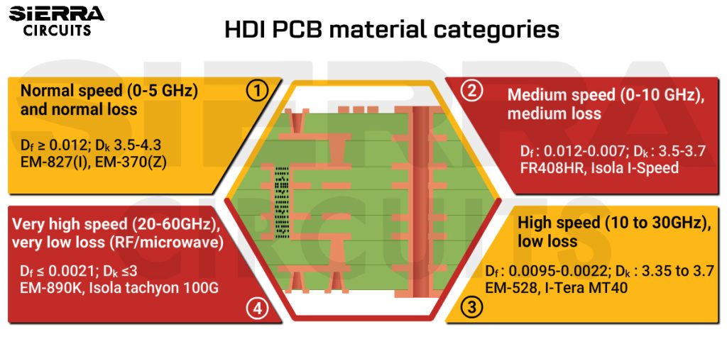
Material selection
Material selection is important for every circuit board design. But we must say it is more important for HDI boards. The designer’s goal is to select the right material for manufacturability, at the same time, meet the temperature and electrical requirements. The physical thickness of the material is important when considering the aspect ratio of the microvia to be plated.
Capping of vias
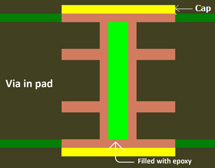
Always fill/cap the microvias to provide a planar copper surface. It also allows easy placement of active parts on both sides of the board. Ignoring this will result in air bubbles and will cost you in the solder joint quality.
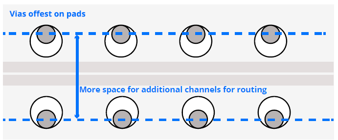
An offset microvia grid
It allows via-in-pad design. Such microvias can be centered in, offset from, or tangent to surface mount pads to provide extra routing.
Reduced plane perforation
Larger power/ground copper area under BGA improves power integrity (PI) and EMC. Wherever microvias perforate a plane; they create a very small gap with minor effects on SI, PI, and EMC. Perforate less to achieve improved image plane effect and higher shielding effectiveness.
Stack-up issues in HDI PCB design
Different layer materials have different CTE values and rates of moisture absorption, which triggers the possibility for delamination. Board designers can avoid it by using the same material for every layer or material with the same CTE value.
Testing
Functional or JTAG test methods are used for HDI PCB design rather than ICT. ICT is definitive but requires full nodal analysis. In the case of BGA that uses blind and buried microvias, you don’t have accessibility unless you bring these to the outer layer(that will violate the signal integrity). If you are using a small-pin package, then you might not have enough space for that.
Thermal management
To provide better thermal management for your design, refer to IPC-2226, which involves thermal issues. Designers need to be more concerned about the thermal issue as the component density of the HDI circuit is high. The thinner dielectrics that go with microvias are an aid to thermal dissipation. In order to maximize the dissipation, consider adding thermal vias.
Wiring demand vs. substrate capacity
Wiring demand is the total connection length required to connect all the parts in the board. The substrate capacity is the wiring length available to connect all the components. The substrate capacity should be larger than the wiring demand so that there will be enough capacity for wiring to complete the design with minimum cost.
Printed wiring board density
Calculate the PWB density to measure the complexity of the design. The amount of density of a printed circuit board (Wd) as measured by the average length of traces per square inch including all signal layers.
The PWB density was derived by assuming an average of three electrical nodes per net and the component lead is a node of a net.
PWB Density (Wd) =β √([Cd] )×(Cc)
=β √([(parts per sq.in.)] )×(ave.leads per part)
Where:
Cd = component density = ave. parts per sq. inch for a design
Cc = component complexity = ave. leads per part
β = Constant, 2.5 for the high analog/discrete region, 3.0 for the analog/digital region, and 3.5 for the digital/ASIC region.
Learn How HDI Boards Can Be More Economical
There is no such thing as universal design rules
“You have to follow only one rule if you are creating a new thing that’s “follow no rules”
Let’s say you’re connecting a micro BGA to a connector and you have to route those connections. The board is 3” by 3” so there are a lot of nets you need to connect in a small space. Is it wrong to design a 4-layer board with 1-mil trace and space of 35 microns just connecting all the nets? Yes, it is. So how do you attack this from a design and manufacturing perspective? There are 2 stack-up decisions you need to make:
- How many routing layers are you going to add?
- How are the routing layers going to be connected?
You should always try to create a stack-up with no less than 3-mil trace and space routing density. If you need a smaller trace and space, please consult the manufacturer whether he can handle less than 3 mil traces. Traces less than 3 mils are much costlier. But start with the 3-mil in mind. Now if you do that… something has to give. Either your board has to be larger or there need to be more layers. So if there’s a space constraint and you need to maintain a form factor then you’re going to be adding more routing layers, which is absolutely fine. Now how are you going to connect these routing layers? Are you going to connect with through-hole vias? Which basically “swiss cheese” all your layers. Or are you going to be able to connect with blind and buried vias that are created by laser drills and free up a lot of that routing space for you?
Option 2 is a much better choice than option 1
And in many cases, option 1 is not even possible. Laser-drilled vias require a much smaller pad size which helps you design faster. And there are plenty of PCB fabricators that can manufacture HDI boards. So once you figure out your minimum routing density required, then you figure out your stack-up, and where your vias are going to start and stop. Sierra Circuits provides a stack-up tool that really gives you a good starting place as to what is a manufacturable design for HDI and what your technology levels are for trace and spaces along with pads and vias.
Other considerations for HDI are what surface finish you choose, what copper thickness you pick, the impedance values, and material types. Try our free HDI tools such as the stack-up Planner and Material Selector. For more information, download our HDI PCB design guide.

HDI PCB Design Guide
5 Chapters - 52 Pages - 60 Minute ReadWhat's Inside:
- Planning your stack-up and microvia structure
- Choosing the right materials
- Signal integrity and controlled impedance in HDI
- Manufacturing considerations for higher yields
Download Now
About Amit Bahl : Amit Bahl, widely recognized as the PCB Guy, earned his Bachelor of Science in Engineering from UCLA. He is currently the Chief Revenue Officer at Sierra Circuits, where he continues to lead efforts to simplify the PCB design journey and support designers and engineers in creating high-quality boards.