Contents

On-demand webinar
How Good is My Shield? An Introduction to Transfer Impedance and Shielding Effectiveness
by Karen Burnham
Choosing the right dielectric material for a PCB is important no matter what application you’re working on. However, the stakes are higher with HDI boards.
High-density materials are categorized into 4 groups: normal speed and normal loss, medium speed and medium loss, high speed and low loss, and very high speed and very low loss. You need to choose the substrates that best suit your design.
Watch the full video to learn how to overcome common challenges in designing HDI circuit boards.
In this article, you will learn how to choose the right dielectric material for your high-density boards.
Highlights:
- The first step in choosing dielectric materials for your high-density board involves identifying the operating frequency and acceptable signal loss.
- For high-speed applications, prioritize materials with low Dk to maximize signal integrity.
- Evaluate the electrical and thermal properties to ensure compatibility with the intended application.
- Verify with your contract manufacturer if the selected laminate is suitable for laser drilling processes.
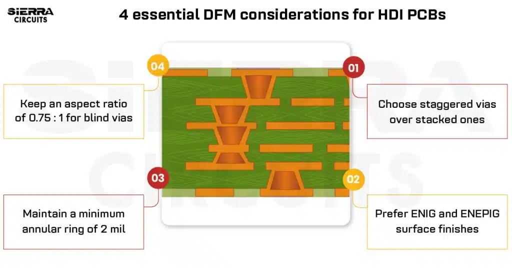
What is a high-density interconnect stack-up?
An HDI PCB features fine lines and spaces (4 mil), microvias, small capture pads (16 mil), and high pad density (>20 pads/cm2). These boards are perfect for small consumer applications.
PCBs mainly consist of polymer resin (dielectric), along with fillers, reinforcement, and copper foil. The image below represents the core material of the PCB sandwiched between copper layers.

To learn more, see how to design an HDI PCB stack-up.
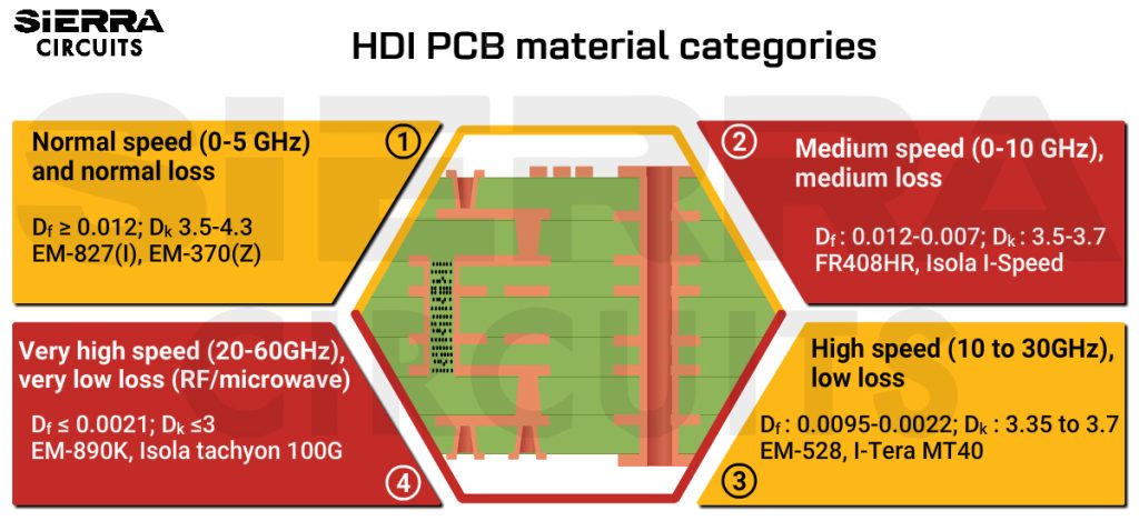
HDI PCB material categories
The first step in selecting dielectric materials for your high-density board is determining the operating frequency (Gbps or GHz) and allowable signal loss (dB).
Next, you need to consider the material’s thermal, electrical, chemical, and mechanical properties.
For instance, high-frequency applications require laminates with a low dielectric loss tangent or dissipation factor (Df) and a flatter Dk versus frequency response curve.
Here’s the classification of high-density circuit board materials:
1. Normal speed and normal loss
These are the most common dielectric materials—the FR4 family. Their Dk versus frequency response is not very flat, and they have a higher dielectric loss.
Therefore, their suitability is limited to a few GHz (0 to 5 GHz). The Df of these materials is greater than 0.012.
EM-827(I), EM-370(Z), Nelco N7000-2HT, and Isola FR370HR are examples of normal speed and normal loss laminates.
2. Medium speed and medium loss
Medium-speed materials exhibit a flatter Dk versus frequency response curve, with approximately half the dielectric loss compared to normal-speed materials.
These dielectrics are suitable for applications operating at 0 to 10 GHz with a dissipation factor of 0.012 to 0.007.
FR408HR and Isola I-Speed fall under this category.
3. High speed and low loss
These materials exhibit lower electrical noise and dielectric loss than the previous 2 categories. They also have a flatter Dk versus frequency response curve.
High-speed and low-loss materials are well-suited for applications operating in the 10 to 30 GHz band. The Df ranges from 0.0095 to 0.0022.
Example materials include EM-528, I-Tera MT40, and Megtron6 R-5775.
4. Very high speed and very low loss (RF/microwave)
Materials for RF/microwave applications have the flattest Dk versus frequency response and the least dielectric loss. They are suitable for applications operating at 20-60GHz. The Df is generally ≤ 0.0021.
EM-890K, Isola Tachyon 100G, and Astra MT77 are very high-speed and very low-loss laminates.
The graph below summarizes the relationship between the signal loss and operating frequency for HDI material categories.

To learn more about HDI design, download our design guide.

HDI PCB Design Guide
5 Chapters - 52 Pages - 60 Minute ReadWhat's Inside:
- Planning your stack-up and microvia structure
- Choosing the right materials
- Signal integrity and controlled impedance in HDI
- Manufacturing considerations for higher yields
Download Now
9 tips for choosing dielectric materials for high-density circuit boards
Once you finalize the material category, you need to consider several other electrical, thermal, and chemical properties of the material. Stick to these guidelines:
1. Select substrates with a low Dk to maximize signal integrity
The dielectric constant is the first thing to consider when comparing different materials for high-density boards. It is the ratio of the material’s electric permeability to the electric permeability of free space (i.e., vacuum).
The dielectric constant also measures the amount of electric potential energy stored in a given volume of material under the action of an electric field.

Dk of most HDI materials ranges from 3 to 4. If you’re working on high-frequency applications, you need to choose a material with a lower dielectric constant, preferably 3 to 3.5.
Select materials with similar dielectric constants to avoid signal integrity issues when using different types of laminates in your circuit board stack-up.


2. Choose densely woven fiberglass to avoid impedance mismatch
Cores and prepregs are made of fiberglass yarn woven into bundles using epoxy resin.
Since the dielectric constants of the fiber and epoxy resin are different, the density of the fiber weaves influences the uniformity of the laminate’s dielectric constant.
Sparsely woven cores and prepregs have non-uniform dielectric constants along the material, causing impedance mismatch and signal loss. The fiber weave structure is important to consider when working with high-frequency applications, as it can cause signal integrity problems.
Opt for densely woven fiberglass weaves such as 1078, 1035, 3313, and 1067 to minimize the fiber weave effect.
3. Pick a dielectric material with low Df to reduce signal attenuation
Df, also called loss tangent (Tan δ), is a metric for quantifying signal attenuation that occurs during signal propagation along a transmission line.
Signal attenuation is caused by the absorption of electromagnetic waves within the dielectric material.
The loss tangent of commonly used dielectric materials ranges between 0.02 and 0.001, and its value increases with frequency. Even minor signal losses in HDI, high-frequency, and high-speed digital applications can result in diminished signal quality.
Select material with a low-loss tangent to reduce signal attenuation, reflections, and localized heating.
4. Employ low-profile copper to minimize conductor loss
Conductor loss is another factor contributing to material losses. It generally occurs due to resistance in the copper foil. For HDI and very high-frequency designs, it’s important to consider the impact of the skin effect on current distribution.
The skin effect phenomenon causes most of the current to be concentrated on the outer surface of the copper conductor. When the frequency reaches a point where the skin depth closely aligns with the roughness of the copper, the current flow is hindered by the unevenness of the copper surface. This results in a rise in resistance and a subsequent increase in conductor loss.

Although surface roughness isn’t usually listed in the datasheets from material manufacturers, a typical value for the outer surface is 3μm, and a typical value for the inner surface is 6μm.
To reduce conductor loss, PCBs should be constructed with wider traces and use rolled copper foils rather than traditional electrodeposited (ED) copper foils.
Panasonic’s Megtron6 is a high-performance laminate with a Dk of 3.4 and Df of 0.004 at 18GHz. This material is offered in standard ED, low, very low, and hyper-low profiles.
5. Use higher Tg and Td laminates to prevent thermal issues
Glass transition temperature (Tg) is the temperature at which the material transforms from solid to viscous. The chosen material’s Tg should be ≥ the maximum withstanding temperature.
For instance, if the operating temperature = 200⁰C, choose a laminate with Tg ≥ 200 ⁰C. Nelco N7000-2HT with Tg = 260⁰C is suitable in this case.
The graph shows that the typical Tg for a standard FR4 material is between 130°C and 140°C, making it suitable for moderate operating temperatures. High-Tg FR4 offers a Tg greater than 170°C. When selecting FR4 for your design, choose the variant that best suits your operating temperature.

If your circuit board operates above Tg, it might soften and lose its mechanical and thermal integrity. This can cause dimensional changes, warping, delamination, mechanical failure, and affect electrical performance.
The glass transition temperature should be higher than the soldering temperature to minimize board stress during assembly.
Decomposition temperature (Td) is the temperature at which the material decomposes chemically. To prevent chemical changes and board degradation, the Td should be significantly higher than manufacturing and operational temperatures.
6. Consider a low CTE material to reduce thermal expansion
CTE (coefficient of thermal expansion) is the rate of expansion of a dielectric material as it heats up. It is expressed in parts per million (ppm) expanded for every degree Celsius that it is heated.
CTE along the X and Y axes is typically between 10 and 20 ppm due to the material’s woven glass structure. This restricts the material’s expansion in X and Y directions, allowing it to expand in the Z direction perpendicular to the surface layer of a circuit board.

Select materials with a CTE that closely matches other components in the assembly. This ensures that the printed board and its components expand and contract at similar rates.
Ideal CTE along the z-axis is 70 ppm or less.
7. Implement a substrate with a high thermal conductivity
Thermal conductivity (k) measures a material’s capacity to transfer heat. This factor determines the heat dissipation rate during operation and its corresponding temperature rise relative to ambient temperature.

Many PCB substrates typically exhibit a thermal conductivity in the range of 0.3 to 0.6 W/m-⁰C, which is relatively lower when compared to copper’s thermal conductivity of 386 W/m-⁰C. Hence, it can be observed that copper layers in your board tend to dissipate heat more efficiently than dielectric material.
Always choose a material with high thermal conductivity to effectively distribute and dissipate heat, protect components from overheating, and prevent localized hotspots.
For more thermal management strategies, see 12 PCB thermal management techniques to reduce PCB heating.
8. Select a material suitable for laser drilling
Evaluate materials based on their ability to withstand circuit board laser drilling procedures and sequential lamination. Choose flat glass clothes with high resin content, such as 1035, 1067, and 1086.
These prepregs have excellent heat absorption properties, allowing for efficient vaporization during laser drilling without compromising structural integrity.
Always check with your PCB material manufacturer to identify options specifically tailored for HDI applications.
To learn about laser drilling, see how laser drilling works in PCBs.
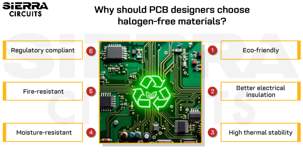
9. Prefer RoHS-compliant substrates
Employ RoHS (restriction of hazardous substances) compliant materials such as lead-free and halogen-free PCB materials. Work with a fab house that avoids the use of toxic materials and implements eco-friendly practices.
To learn more about PCB material selection, download our design guide.

PCB Material Design Guide
9 Chapters - 30 Pages - 40 Minute ReadWhat's Inside:
- Basic properties of the dielectric material to be considered
- Signal loss in PCB substrates
- Copper foil selection
- Key considerations for choosing PCB materials
Download Now
HDI materials cost Vs. performance
The higher the performance, the costlier the material. Here is a chart of common dielectrics comparing the cost to performance, along with typical applications:

Key Takeaways
- When selecting dielectric materials, consider parameters such as operating frequency, signal loss, thermal, electrical, chemical, and mechanical properties.
- Higher frequency signals require materials with lower dielectric constants and low-loss tangents to minimize signal attenuation.
- Glass transition temperature (Tg), decomposition temperature (Td), coefficient of thermal expansion (CTE), and thermal conductivity play vital roles in ensuring material reliability and effective heat management.
- Higher-performing materials often come at a higher cost. It’s essential to balance material costs against performance requirements.
Selecting the right dielectric material for high-density interconnect PCBs is paramount for ensuring optimal performance and reliability in electronic products. By considering operating frequency, signal loss, thermal, electrical, chemical, and mechanical properties, you can make informed decisions when selecting the right substrate.
About the author: Atar Mittal is the Director and General Manager of Sierra Circuits’ design and assembly division. He is responsible for designing and developing strategies and process automation tools for complex printed circuit boards and assemblies. Atar is also currently developing productivity tools for electronics designers that would greatly shorten development time.
Need assistance in selecting material for your high-density board? Post your queries on our PCB forum, SierraConnect. Our design and manufacturing experts will help you select one.

About Atar Mittal : Atar Mittal is the General Manager and Director of the Design and Assembly Sierra Circuits division. He has a degree in Electrical Engineering from IIT Kharagpur and has worked in the electronics industry for over three decades.