HDI PCB Design Guide
Sierra Circuits’ HDI PCB Design Guide helps you design high-density circuit boards for improved routing density, electrical performance, and manufacturability.


The HDI PCB Design Guide is updated with new recommendations from industry experts. It provides practical guidance on selecting materials, developing stack-ups, choosing via structures, and routing fine-pitch BGAs.
Key topics include signal integrity, power delivery, thermal management, DFM/DFA, and manufacturing tolerances.
Here’s a quick breakdown of what you’ll learn in this guide:
- Why and when to choose HDI technology
- How to plan an HDI design before starting your layout
- How to select materials based on electrical, thermal, and manufacturing requirements
- How to develop HDI stack-ups and choose the appropriate build-up structure
- How to select the right via structure (blind/buried/microvia/via-in-pad)
- DFM and DFA considerations
- How to design power distribution networks and manage thermal performance
- How to choose the right BGA breakout strategy for fine-pitch devices
- What manufacturing tolerances to consider for drilling, annular rings, traces, impedance, copper, and solder mask
The following sections provide a closer look at what you’ll learn in the guide.
Why choose HDI technology for your PCB?
As electronic products become smaller and more capable, PCB designers need to accommodate more components, higher pin counts, faster signals, and greater functionality within increasingly limited board space.
HDI technology addresses these challenges through advanced interconnect structures and sequential lamination. These technologies allow designers to create dense routing structures while using board space more efficiently.
The guide emphasizes an important question to ask early in the design process: Will HDI solve a real problem and serve a clear purpose in the design?
High-density technology is particularly useful when your design includes fine-pitch, high-pin-count packages, high-speed signals, or multiple functions that need to fit within a compact area.
For example, fine-pitch BGAs, CSPs, flip-chip BGAs, COBs, and SiPs can be difficult to route using conventional PCB technology without increasing board size or layer count. HDI provides additional routing density to accommodate these packages.
For high-speed designs, microvias can also reduce via stubs and parasitic effects, improving electrical performance.
The key is to determine why you need HDI before you start your project.
How to build a stack-up for high-density boards?
Material and stack-up selection directly affect the overall performance, reliability, manufacturability, and cost of a high-density board.
The selected material should meet the electrical requirements and withstand processes such as laser drilling, microvia formation, sequential lamination, and repeated thermal cycles.
Key properties to consider include dielectric constant (Dk), dissipation factor (Df), glass transition temperature (Tg), decomposition temperature (Td), coefficient of thermal expansion (CTE), thermal conductivity, fiberglass weave, copper profile, moisture absorption, laser-drilling compatibility, and material availability.
For high-speed designs, a low and stable Dk can support signal integrity and impedance control, while a low Df helps you minimize signal loss and dielectric heating.
Laminate selection should also account for dimensional stability and material movement during complex manufacturing processes. Once the material is selected, the stack-up must be designed based on factors such as BGA pitch and pin count, signal breakout requirements, power/ground needs, and manufacturing capabilities.
Common HDI architectures include 0-N-0, 1-N-1, 2-N-2, and 3-N-3, which indicate the number of sequential build-up layers on either side of the core. As the number of build-up layers increases, fabrication becomes more complex because of additional lamination, drilling, plating, imaging, registration, and inspection requirements.
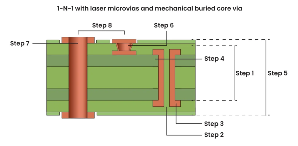
A balanced, symmetrical stack-up can prevent warpage. Choosing the simplest structure that provides the required routing density and electrical performance can also reduce cost and improve manufacturability.
How to strike a balance between HDI performance and cost?
High-density interconnect is often considered a more expensive technology because it involves laser drilling, sequential lamination, via filling, and tighter process controls.
The HDI PCB design guide emphasizes selecting the simplest architecture that meets the routing and electrical requirements. Each additional process adds to manufacturing complexity and can increase cost and yield risk.
For example, a 0-N-0 structure avoids sequential build-up layers and is one of the simpler HDI structures. A 1-N-1 structure adds one sequential build-up layer on each side of the core, while 2-N-2 and 3-N-3 structures introduce progressively more build-up layers and manufacturing complexity.
The objective isn’t to use the most sophisticated technology available. It is to use the right one for your design.
Which via structure should you use in high-density designs?
Vias are one of the most important design decisions. The guide covers the different hole structures used to achieve higher routing density, including microvias, blind vias, buried vias, through-hole vias, stacked microvias, staggered microvias, via-in-pad, and every-layer interconnect structures.
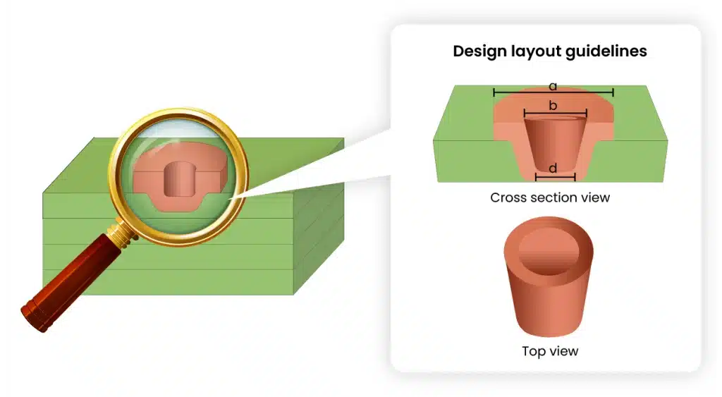
Microvias are particularly important because they connect adjacent layers without extending through the entire board. Their small size frees up routing space and can reduce via stubs.
The HDI PCB design guide recommends keeping the microvia aspect ratio at 0.8:1 or lower whenever possible to improve plating quality. It also recommends validating via dimensions, capture pads, annular rings, and stack-up with the PCB manufacturer early in the design process.
Stacked vs. staggered microvias
The choice between stacked and staggered microvias depends on routing density, signal requirements, manufacturing capability, and available space.
Staggered microvias are generally preferred when they can provide the required routing density without introducing unnecessary manufacturing complexity. Stacked microvias can be useful when space is extremely limited, particularly in dense BGA breakouts.
For ultra-high-speed designs, the guide also discusses how via structure can influence signal discontinuities and controlled impedance.
How does HDI improve signal integrity and return-path performance?
Signal integrity becomes increasingly important as rise times decrease and operating speeds increase. High-density technology can improve signal integrity by reducing the electrical distance between components, shortening signal paths, and minimizing parasitic inductance and capacitance.
Smaller vias, shorter traces, thinner dielectric layers, and closer component placement contribute to shorter electrical paths. Microvias also reduce via stubs, which can introduce discontinuities at high frequencies. At the same time, closely spaced reference planes and shorter current paths can improve return-path performance by reducing loop inductance, switching noise, and electromagnetic interference (EMI).
However, HDI does not automatically guarantee good signal integrity. Designers still need to carefully manage trace geometry, via transitions, return paths, reference planes, dielectric materials, controlled impedance, crosstalk, and signal discontinuities. Properly placed vias can also reduce inductance, minimize disruption to copper planes, and improve power delivery.
The HDI PCB Design guide provides practical guidance on these design considerations to help you achieve reliable high-speed performance with HDI technology.
How to manage power delivery and thermal performance in high-density interconnects?
As component density and power consumption increase, power integrity and thermal management become increasingly important.
Processors, FPGAs, DDR memory, and high-speed interfaces can demand significant transient currents while operating at lower supply voltages. A well-designed power distribution network (PDN) provides stable voltage with minimal noise, voltage drop, and impedance.
HDI printed boards can improve power delivery through shorter current paths, smaller vias, thin dielectric layers, and closely spaced power and ground planes. Via-in-pad structures can further minimize connection lengths and provide lower-inductance connections.
When it comes to thermal management, the guide recommends distributing heat-generating components rather than clustering them unnecessarily. Place thermal vias beneath exposed thermal pads and connect those vias to internal copper planes to maximize copper area around high-power devices.
Material selection also matters. High thermal conductivity, low CTE, high Tg, and stable dielectric properties can be important for high-density boards operating at elevated temperatures or carrying significant power.
How do you choose the right BGA breakout strategy for HDI PCBs?
Fine-pitch BGAs are one of the primary reasons designers turn to high-density technology.
As BGA pitch decreases and pin count increases, conventional dog-bone routing can consume the available routing space. Microvias, via-in-pad, blind vias, buried vias, and fine traces provide alternative ways to escape signals from dense BGA packages.
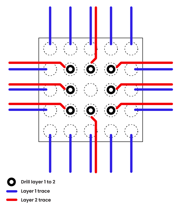
The HDI PCB Design guide compares three common BGA breakout approaches: via-in-pad, microvias, and dog-bone routing. Via-in-pad provides the highest routing density and is typically used for BGA pitches of 0.5 mm or smaller.
Microvias offer high routing density and are commonly suited for 0.4 mm to 0.5 mm BGAs, while providing good signal integrity with moderate fabrication complexity.
Dog-bone routing is generally used for larger-pitch BGAs, typically 0.8 mm and above, where routing density is less critical, and simpler fabrication is preferred. The right approach depends on the BGA pitch, routing requirements, signal integrity needs, and manufacturing capabilities.
When should you use via-in-pad?
Via-in-pad places the plated hole directly within the component pad. This can minimize trace length, reduce parasitic inductance, eliminate via stubs, and provide the routing density required by fine-pitch packages.
For vias placed directly in component pads, the guide recommends using filled and capped structures to prevent solder wicking and ensure reliable solder joints.
When should you use microvias?
Microvias provide high routing density and require less space than conventional vias. They are commonly used for BGA pitches in the 0.4 mm to 0.5 mm range.
When does dog-bone routing make sense?
Dog-bone routing uses a short trace to connect the BGA pad to a via located outside the pad.
It is generally easier and more economical to manufacture but consumes more routing space and introduces via stubs. The guide recommends dog-bone routing for larger-pitch BGAs where manufacturing simplicity and cost are more important than improving routing density.
Why follow DFM guidelines for HDI designs?
HDI designs have tighter manufacturing margins than conventional multilayer boards.
Fine traces, small pads, microvias, complex stack-ups, and tight registration requirements all increase the impact of manufacturing variation.
DFM is particularly important during the design process, as even small variations can affect manufacturability.
A thorough design review should be performed before the layout is finalized.
You should verify trace width and spacing, microvia aspect ratio, annular rings, via-in-pad structures, stack-up symmetry, surface finish, solder mask clearances, and fabrication tolerances against the manufacturer’s capabilities.
HDI technology gives designers more freedom to build smaller, denser, and higher-performance electronics. But achieving those benefits requires careful decisions at every stage of the design.
Download the HDI PCB Design Guide to get practical guidelines from industry experts.