


Contents

On-demand webinar
How Good is My Shield? An Introduction to Transfer Impedance and Shielding Effectiveness
by Karen Burnham
Staggered and stacked vias are well adapted nowadays. Their unique design enhances the density, as well as boosts the signal integrity and routing flexibility. By incorporating staggered and stacked vias in your design, you can get a compact, efficacious circuit board.
For the last few decades, the entire electronic industry has been changing rapidly. The revolution in the technical field induces greater use of high-density interconnection (HDI) boards. HDI makes provision for a greater number of small components in a dense region with versatile routing and high-performance capability. Usually, there are 120-160 pins per square inch in these boards. The microvias, i.e., staggered and stacked vias, are highly associated with this type of design. In this article, we will analyze the design specifications and constraints, and also explore the reliability factors of staggered and stacked vias.
What are microvias?
Staggered and stacked vias are different types of microvias. Before jumping into the definition and details of this, here’s an overview of microvias.
Microvias provide connections between layers in a multilayer board. They have smaller diameters than mechanically drilled holes. This enhances the routable area on a board. Primarily, they are the miniature version of a conventional via, except for the structure. If your design requires advanced, close-packed circuitry, microvias are the best choice. They are quite appropriate for high-speed designs because of their lower parasitic capacitance.
Apart from making the board light in weight and compact in design, microvias have many advantages.
- Superior electrical performance
- Improved signal integrity
- Lower EMI/RFI and crosstalk
- Smaller size and weight
- Optimizes the overall cost
- Reduces design completion time
- Increases reliability
Microvias are created by laser drilling
Laser drilling is a suitable method for fabricating microvias to achieve a high-density design with shorter traces. In this case, a laser beam vaporizes the drill area (as per the drill file) and creates holes.
The critical parameters in this process are the pad size, the laser drill size, and the press-out thickness of the dielectric. You must keep your laser drill size in proportion to the finished press-out thickness of the dielectric layer to plate the via adequately. For more details on laser drilling, see How does Laser Drilling Work in PCBs?
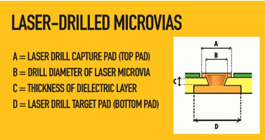
After the completion of drilling and deburring, the plating process is carried out with electrolytic deposition or the electroless copper plating technique.
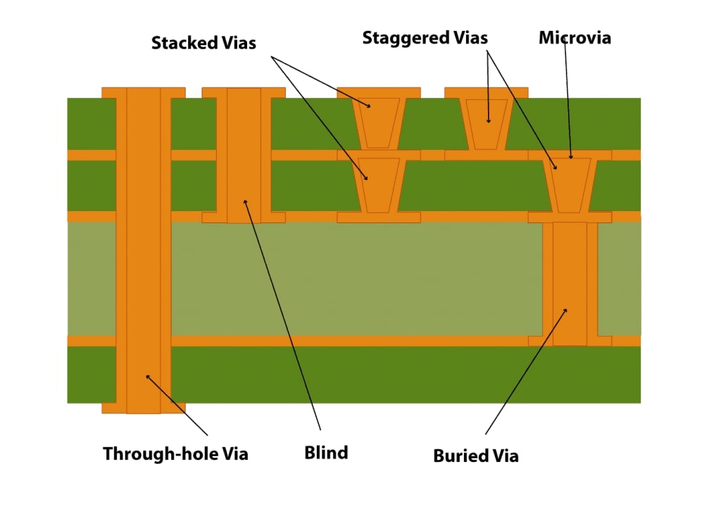
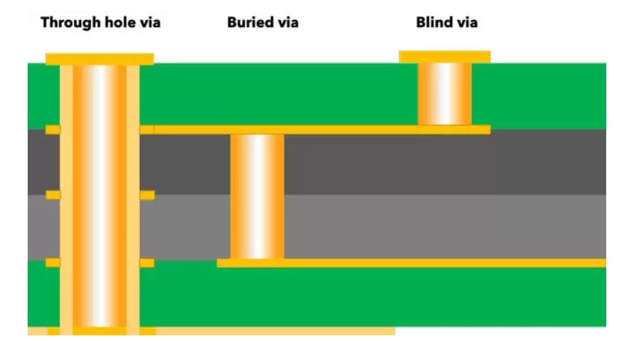
The fundamentals of blind and buried vias
The staggered and stacked vias implement the concept of blind and buried vias. Blind vias make a connection between one outer layer and at least one inner layer. It always passes through either the top or bottom layer of the board, but does not pierce through all the layers in the circuitry. Hence, it is hidden from one side.
Buried via does not have a connection with any of the outer layers. It is completely veiled from the outside. This type of via passes through any number of inner layers. These are electroplated holes and require a separate drill file.
Calculating the right aspect ratio
Aspect ratio is considered a critical factor while executing laser drilling. It is a parameter used to measure the reliability of a via and set the manufacturing limitation.
From a mathematical perspective, an aspect ratio is a ratio of drill depth to drill diameter:
AR= h/a
Where,
h = (Outer dielectric thickness + Copper foil thickness)= Hole depth
a = Microvia diameter

The requirement of plating is proportional to the aspect ratio. More plating increases the risk of rupture because of the expansion during the assembly process. Lower AR ensures even plating, superior electrical connection, and provides great mechanical strength. IPC defines microvia as perfect when they have a 1:1 aspect ratio, whereas microvias having a 0.75:1 aspect ratio are the standard ones.
The ruling factor of HDI design is to achieve absolute reliability and supreme quality. In 2019, IPC issued a warning that the larger the aspect ratio, the greater the possibility of design failure during reflex cycles. It is better to use a larger via diameter or a thinner copper foil, and even both can be a good choice. Suitably, a 6 mil diameter is good enough to withstand several thermal cycles.
For more, download the PCB Via Design Guide.
PCB Via Design Guide
7 Chapters - 90 Pages - 70 Minute ReadWhat's Inside:
- Guidelines for choosing the right via for your application
- Design rules for advanced via structures
- DFM tips to avoid manufacturing errors
- Signal integrity considerations for high-speed designs
- Testing and inspection methods for via reliability
- Fab notes
Download Now
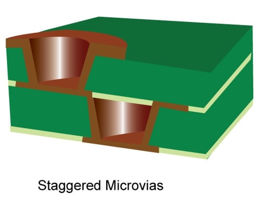
What are staggered vias?
Staggered vias connect different layers of the board but do not come in direct contact with each other (separate drill axis). Their position is offset on the adjacent layers. Staggered microvias involve fewer design steps. As the second drilled hole is not adjoined with the first one, the laser-drilled vias do not need copper filling. Hence, the design comprises less complicated but time-consuming processes.
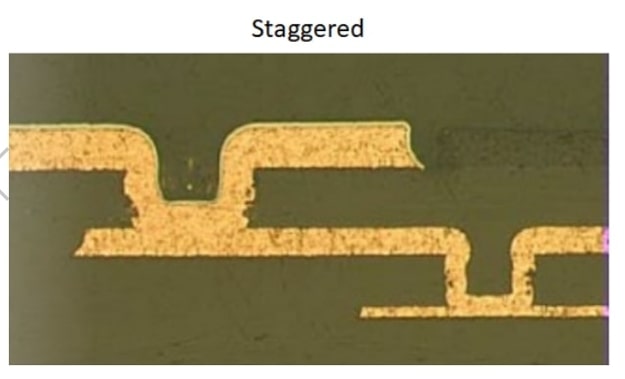
The spacing between the laser-drilled holes is the most primitive concern while designing a staggered via. The vertical distance between the centers of two microvias decides whether the staggered via design is possible or not. The vertical separation should be greater than the microvia diameter to arrive at a perfect staggered design.
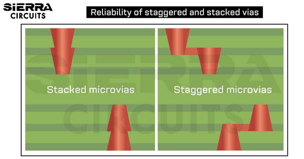
Reliability of staggered vias
When multiple microvias are stacked, it exerts stress on the via walls. This can detach the topmost via from the pad. Therefore, the staggered configuration is preferred over the stacked configuration when you have to connect more than 2 layers using microvias.
However, staggered via is not the right choice when your design demands space constraints. This is because they require more space on the board with less complexity. The crosstalk issue is negligible since microvias are placed offset from each other.
Staggered vias tend to introduce some discontinuity in the path between source and destination. Therefore, they can not meet the requirement of uniform via impedance. This fact makes them undesirable in ultra-high-speed designs.
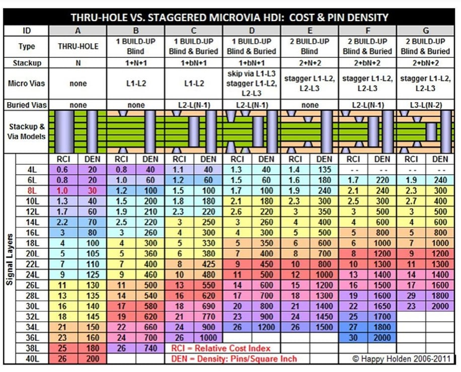
The table shows the comparison between staggered via and through-hole via in terms of cost and pin density.
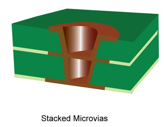
What are stacked vias?
Manufacturing a board using stacked vias involves more steps than staggered vias. Therefore, it is more complex. Here, several vias are stacked on top of each other. They connect different layers and occupy less space. Every via is drilled and plated before stacking on top of another. There are two narrow annular rings on the top and the bottom. The upper one signifies the precise registration, and the bottom one is used for electrical connection. The design consists of three different actions:
- Hole filling with copper
- Planarization
- Extra imaging
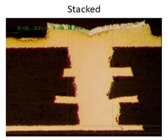
Copper filling of stacked vias
The stacked vias are filled with electroplated copper. It ensures a solid electrical connection and provides structural support. There are occasions when defects can be seen in the deposited copper. Some obstacles are explained below:
- The improper deposition of copper can create voids in the vias. These voids generate localized stress within the structure. This can hamper the reliability of the stacked microvias.
- Low-grade electroless copper results in inferior bonding between the base of the microvia and the target pad under it.
Read our case study on designing 8- and 14-layer HDI PCBs with stacked vias to know about the challenges that we faced while designing and how we solved them without compromising the design and manufacturing standards.
Reliability of stacked vias
The primary advantage of stacked vias is their compactness. In HDI circuit boards, the practical routing of stacked vias ensures flexibility. Moreover, controlled impedance is well maintained from the signal source to the load destination.

The reliability is impacted when pressure is exerted on the microvia from the z-axis of the dielectric. This occurs due to a mismatch of CTE of materials. Beyond the glass transition temperature (Tg), dielectric expands 200 parts per million, whereas copper expands up to 16 parts per million. Hence, as long as there is a single microvia involved, everything is sorted. But when the layer increases to two, the discrepancy starts to occur. As the layer count goes to three, the mismatch goes beyond tolerable limits. Consequently, failure happens due to corner cracking or barrel cracking.
Stacked vias vs. staggered vias
| Parameters | Stacked vias | Staggered vias |
|---|---|---|
| Via arrangement | Microvias are stacked on top of one another | Here, the vias are positioned offset on the adjacent layers with separate drill axes |
| Filling requirement | Should be filled with electroplated copper to ensure electrical connectivity | Only the vias connected to the external layers require conductive filling |
| Space constraint | Occupy less space | Require more room on the board as vertical distance between two vias should be greater than the drill diameter |
| Crosstalk issues | Risk of crosstalk is more as they are placed on the same drill axes | Less crosstalk as the microvias do not come into direct contact with each other |
| Controlled impedance | Uniform trace geometry aids in achieving controlled impedance | Signal transmission path encounters impedance discontinuity due to offset vias |
Stack-up with staggered and stacked microvias
High-density board stack-ups involve staggered and stacked microvias as per the requirements of the design. According to IPC-2226, an HDI PCB stack-up comprises various standardized steps.
i+N+i stack-up
The structure is defined as an i+N+i stack-up. Here, ‘i’ represents the number of sequentially laminated layers connected with microvias in the outer parts. The inner sections are coupled with the top of the outer parts. The middle core is connected with buried vias. These buried vias are connected to the inner layers further.
The number of sequential laminations can be anything, as per the design specification fixed by the fabrication team. Technically, there is no proper limit to N, though it depends on the layer count and the outer layer thickness. The 1+N+1 stack-up is the simplest one without microvias. The fabrication house can have options like 2+N+2, 3+N+3, and 4+N+4 stack-ups incorporating staggered and stacked vias.
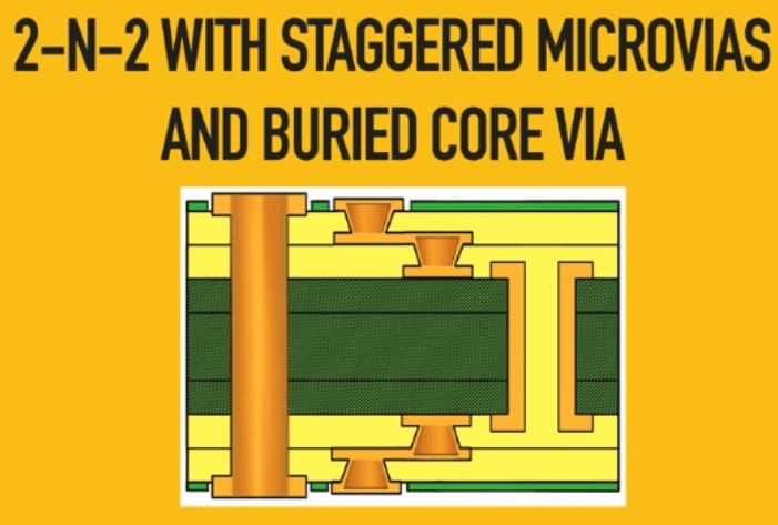
2+N+2 stack up
The most commonly used stack-up is 2+N+2. It provides mechanical support with fewer pins and moderate high-density BGA components. There are multiple sequentially laminated HDI layers and one conventional inner layer to complete the stack.
To learn how to reliable build high-density boards, download the HDI PCB Design Guide.

HDI PCB Design Guide
5 Chapters - 52 Pages - 60 Minute Read
What's Inside:
Download Now
Sequential lamination
Staggered and stacked microvias follow the sequential lamination process. In the fabrication process, a layer of epoxy pre-impregnated fiberglass sheet is sandwiched between copper layers. Next, the lamination is performed under high temperatures and high hydraulic pressure. Sequential lamination involves adding a dielectric layer between the copper and the laminated sub-composite layer.
This is used multiple times to incorporate various combinations of layer stack-up and via structure in complex HDI designs.
Staggered and stacked holes improve signal integrity
Staggered and stacked microvias improve signal integrity by reducing the size and offering small current loops on critical nets. They reduce stub lengths and thus the effects of the signal reflection will be mitigated. The various types of noise that can be avoided using staggered and stacked vias are mentioned below.
Switching noise
The physical structure of staggered and stacked microvias is unique. They are small and short. These kinds of vias have almost one-tenth as much electric parasitics as mechanical through-holes. The configuration helps in decreasing inductance and parasitic capacitance and thus reduces switching and circuit noise.
Crosstalk and EMI
The staggered and stacked vias provide superior resistance to crosstalk and EMI in a PCB design. The shorter interconnect length reduces the crosstalk by a noticeable amount as it radiates less. If the length and dielectric thickness are reduced by half, the crosstalk can be reduced by almost one-fourth from the conventional via. Additionally, less distance from the reference plane also contributes to mitigating crosstalk. The routable area also increases, which further decreases electromagnetic interference (EMI) and crosstalk.
Staggered and stacked microvias can withstand many thermal life cycles. The signal integrity arrives at a remarkable level by making them useful in complex, dense designs. Sierra Circuits delivers high-quality board designs involving staggered and stacked vias. We always give primary importance to customers’ specifications and try to provide the best-performing circuit without violating the constraints of these types of vias. If you have any queries regarding this, do drop a comment below.

About Poulomi Ghosh : Poulomi is a microwave engineer specializing in EMI, EMC, RF, and high-speed electronics. As a senior technical writer at Sierra Circuits, she creates advanced engineering articles and webinars for hardware engineers and PCB designers.


