Contents
What can be more problematic than seeing your expensive PCB not performing as intended? What would you do if your expensive circuit board failed in the production line even after accurate prototyping and thorough testing? One of the common reasons for PCB failure is ionic contamination due to its exposure to dust, moisture, and the environment.
If not treated properly, ionic contamination can cause PCB corrosion, electromechanical migration (ECM), dendrite formation, and parasitic leakage. To ensure reliability and avoid rework and late life cycle failures, the PCBs are tested for ionic contamination. Ionic contamination testing is performed through ROSE and ion chromatography tests. The ionic contamination analysis for any PCB should be done under the set IPC standards.
The growing use of PCBs in harsh environments, specifically in safety-critical applications, requires adequate electrochemical reliability to control ionic contamination. The production of circuit boards includes at least 20 chemical processes, and most of them involve extensive use of ionic matter. Contaminants can be ionic and non-ionic residues. Non-ionic residues are oils, resin, and grease. They don’t have conductive properties to remain on the PCB surface after PCB assembly. On the other hand, ionic contaminants can be salts, organic/inorganic acids, flux activators, and plating chemistries. To maintain a quality manufacturing process, it is very important to identify and control them. In this blog post, we will be discussing ionic contamination only.
What is ionic contamination in a PCB?
Ionic contamination issues arise due to the ionic residues left behind during PCB fabrication and assembly processes. These residues can be plastic, metal, and fiberglass granules, including salts, oils, and dust. These ionic residues have a zero net charge (the composition of positive cations and negative anions) and become charged when a PCB passes through multiple fabrication processes. During assembly, the components also carry various ionic/conductive contaminants along with cutting oils/fluids, biocides, and corrosion preventatives. How do we handle circuit boards in the production line is also a major cause of ionic contamination in a PCB.
Sources of ionic contamination in a PCB
Ionic contamination may occur during PCB fabrication and assembly processes. During fabrication, the creation of PTHs, etching process, and drilling are responsible for the contamination. On the other hand, during assembly, flux residue in soldering, component biocides by pick and place machine, and ionic surfactants from solder preparation are responsible for PCB ionic contamination. Read the post on component placement guidelines for PCB design and assembly.
- Moisture trapped in PCB layers: Ionic contaminants in contact with moisture can increase short-circuit risk.
- Etching chemicals: Chemicals used for PCB etching purposes are highly conductive and corrosive. It is essential to neutralize/rinse them since they can be a potential cause of leakage current.
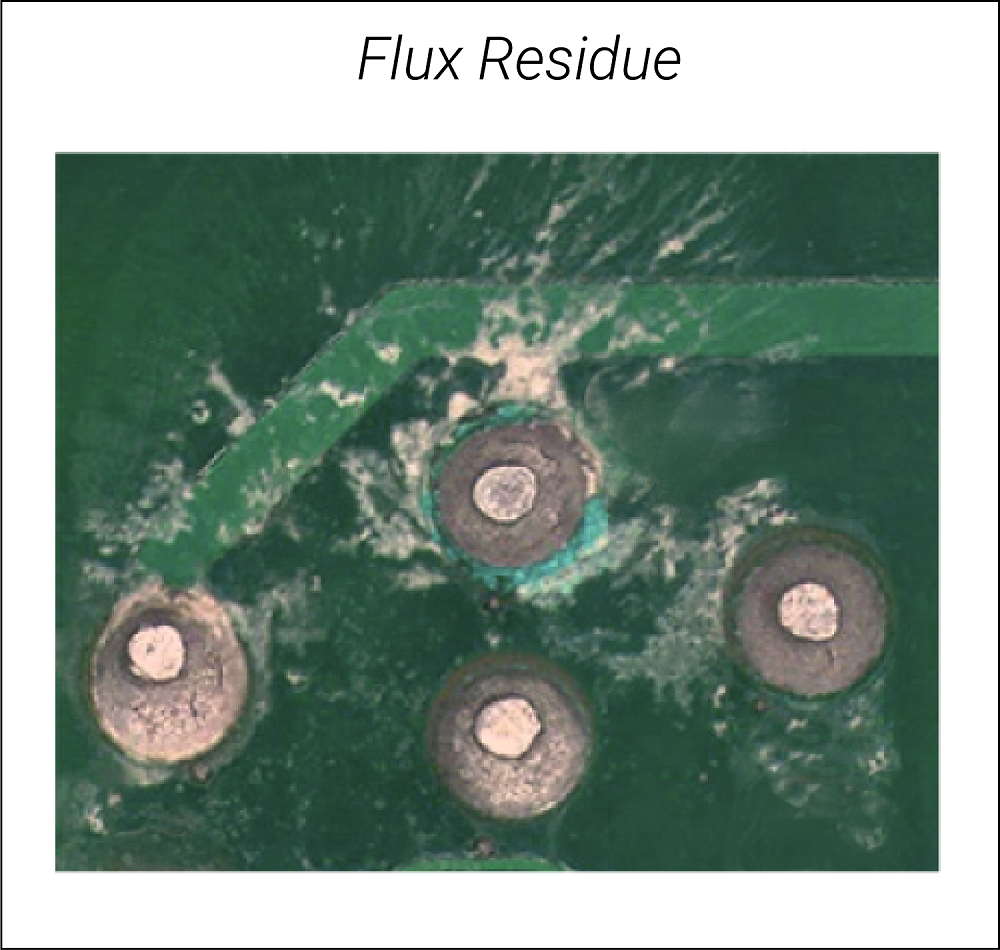
- Flux residues: Common conductive flux residues from the soldering process include various unreacted activators, binders, rheology components, and saponifiers. These residues must be removed by using solvent cleaning, say vapor degreasing, or by aqueous chemistries in the common batch.
- Inter-layer residues during drilling and plating (PTHs): Inter-layer residues generated during drilling and plating are also responsible for ionic contamination.
- Improper PCB surface cleaning: The majority of ionic contaminants come from the board itself. Before placing components over the bare board, you need to ensure that no contaminant is left from the previous production step.
Effects of ionic contamination in a PCB
The occurrence of ionic contamination on PCB assembly can inhibit its performance. In the production house, bare boards can carry ionic contaminants in the form of left-over flux, etching chemical, and solder material. If these residues are left on the board, major issues, like Electrochemical Migration (ECM), corroded traces, parasitic leakages, and dendritic growth, can hamper the PCB’s life-cycle. Read 8 soldering tips to avoid possible ionic contamination issues.
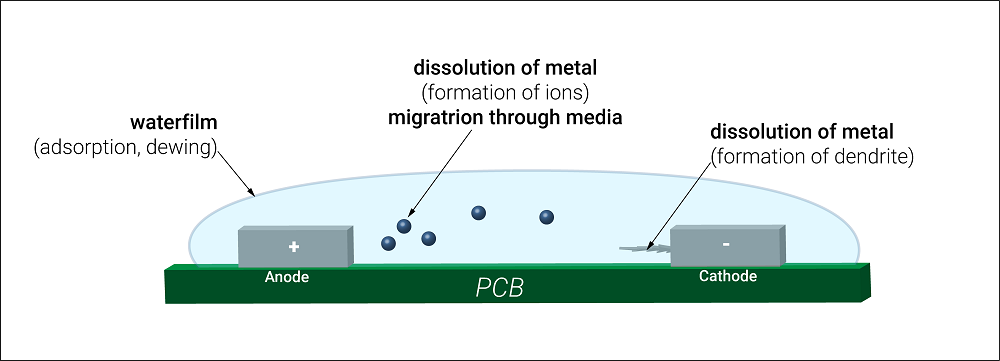
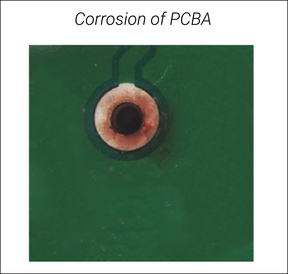
- Electrochemical migration (ECM): Electrochemical migration is caused by the electric field in which metal gets dissolved, resulting in ion formation between two copper features. If the electric field is applied, the metal dissolves at the Anode and gets deposited to the Cathode resulting in dendrite growth. Because dendrites grow from conductive ions, they can direct PCB currents differently from what is intended, leading to short circuits. Dendrites create alternative current paths that can affect the accuracy of current measurements in a PCB.

- Corrosion: Usually, PCBs corrode due to their material. Ionic contamination can corrode the entire PCB in a much shorter time. When ionic residue comes in contact with moisture, the short-circuit risk increases. The corroding metal flakes off, overlooking the chemical properties needed for the PCB to operate correctly. Selecting apt PCB material and laminates help with ionic contamination issues.
Ionic contamination alone is not responsible for the above consequences; moisture and environmental exposure are also. That is why PCBs are baked to eliminate moisture before starting any new process. The ionic contamination level needs to be controlled during the manufacturing of circuit boards by adopting a process control tool. This tool ensures that the individual production process steps (e.g., surface-mount or through-hole) are performed in a controlled manner to achieve a manageable ionic contamination level.
The why’s and the how’s of keeping your PCB clean
A PCB in the outside world is exposed to harsh environmental conditions such as humidity, temperature changes, chemicals, etc. The use of PCB casing, solder mask, and isolation equipment may reduce the effect of environmental factors. However, the accumulation of ionic residues during fabrication and PCB assembly can accelerate ionic contamination. Ionic contamination may also be caused due to the lack of board cleanliness.
IPC TM 650-2.3.25 describes how to perform ionic contamination testing for circuit boards. These tests also determine the types of impurities on board assemblies and components and their acceptable limits.

IPC Class 3 Design Guide
8 Chapters - 23 Pages - 35 Minute ReadWhat's Inside:
- IPC guidelines for manufacturing defects
- IPC standards for assembly processes
- Common differences between the classes
- IPC documents to set the level of acceptance criteria
Download Now
Ionic contamination testing in a PCB
Bad quality control during PCB fabrication, component placement, and a sub-standard final cleaning are some of the major issues responsible for ionic contamination. It is crucial to identify, control, and mitigate such issues. This can be done with proper ionic contamination testing equipment and analysis. ROSE testing, ion extraction, and ion chromatography are some of the well-known methods. Sometimes, humidity validation testing is also performed at the beginning of the production.
To ensure the life-span of the PCB, testing of the bare board for ionic contamination prior to assembly reduces the risk of defects caused by contaminants. Ionic contamination testing is performed to detect ionic residues resulting from the fabrication and soldering steps. Let’s have a detailed analysis of cleanliness testing methods for the determination of ionic contamination.
The Resistivity of Solvent Extract (ROSE) test
The widely used ROSE test determines ionic bulk, which is responsible for the contamination. The ROSE test measures the ions found on the PCB that is dipped into a solvent solution. The test results are measured in bulk ions per square inch. The following diagram shows a ROSE test:
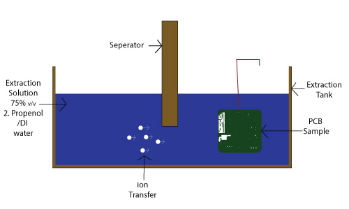
As per the IPC 650-2.3.25 standard, the ionic contamination test specimen is used as per the equipment manufacturer’s recommendations. Calculations for the bare-board and assembled boards are also given in the standard.
Length x Width x 2 = Unpopulated Board Surface Area
(Length x Width x 2) + up to 50% = Assembled Board Surface Area
The selection of the solution is done as per the specifications given by the equipment manufacturer. The industry has established two different standard test solutions that are used worldwide:
75 % v/v 2-propanol/DI water
50 % v/v 2-propanol/DI water
Several changes have been made to ROSE testing over the years in terms of equipment, testing procedure, types of chemicals used, and more. The ROSE test was reiterated with the addition of thermal extraction methods and called a modified ROSE test. Similar to the standard ROSE test, it involves an exchange of bulk ions between a PCB and solvent. A modified ROSE test is carried out at an elevated temperature to accelerate ion transfer. The modified ROSE test is performed in ionograph-style equipment.
Test report 1:
Ionic cleanliness test or ROSE test determines the conductivity or resistivity of a PCB sample. The ionic contamination tester is used along with the combination of isopropyl alcohol (IPA) and deionized water. The ionic tester collects a sample of possible residues present on the board. The residue is deployed for resistivity (conductivity) testing, which indicates the board’s soil levels.
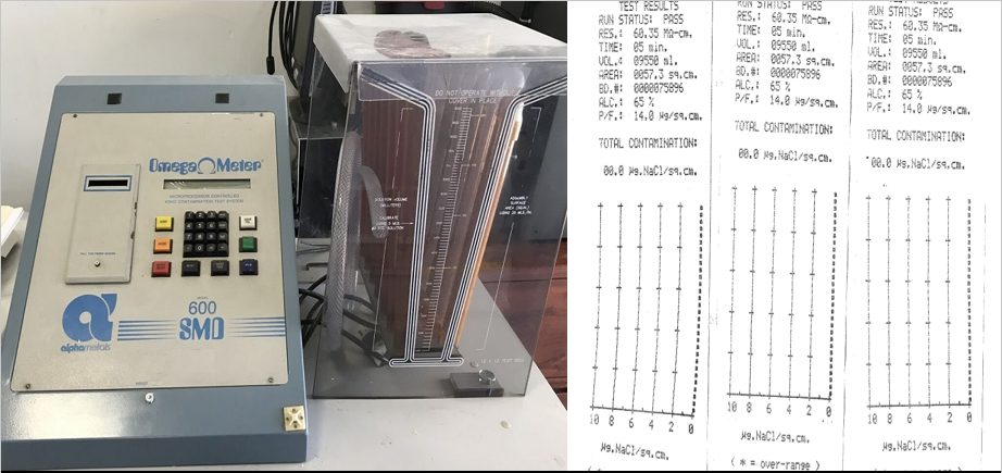
The test results provided by OMEGA 600 SMD of the final contamination level are predetermined as per IPC TM 650 and MIL-P 28809 (for military applications). The Omega Meter registers higher values compared to the Contaminometer. For bare boards or non-assembled boards, the permitted contamination level is less than 0.0001 mg/cm2 NaCI equivalents, while for the hand-soldered assemblies, the permitted contamination level is about 0.0003 mg/cm2 NaCl equivalents. For PCB assemblies with a dispensed rosin-based solder paste, the permitted contamination level is 0.0003 mg/cm2 NaCl equivalents.

Test report 2:
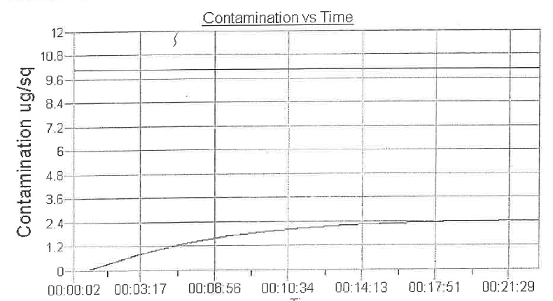
Ionographs are used to perform dynamic testing of ionic contamination. These systems use an ultra-pure alcohol/water extraction media and a ‘dynamic method’ to test product samples quickly and non-destructively. Ionographs measures the quality of electronic components and circuit boards before flux application, thus avoiding encapsulation of contaminants. This method also monitors the level of no-clean flux applied during spray or foam fluxing to help avoid electrical failures due to excessive flux deposits. It also discovers solder defects caused by insufficient flux.
To understand the ionic impurity, the measurements have been taken considering per square inch of the board. The results are measured in NaCl (sodium chloride)/square inch present on the board. The fail point is the maximum allowed ug NaCl per square inch as per the IPC standards. It is based on the size of the board dimension entered.
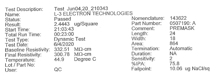
The above testing report lists the customer, results in ug/sq” of NaCl, start time, run time, test date, baseline or starting resistivity, final resistivity (to determine cleanliness/contamination level), the temperature of the bath, lot number when required, tool number, customer part number, premask or final, board dimensions, automatic time termination of the test, the sensitivity of the test, and IPA % (will always be around 75%).
The machine self-calibrates to a base resistivity then the sample is inserted to check the change in resistivity over a period of time. It determines the ionic contamination/cleanliness level as long as it is under 10.06 ug NaCl/sq (the fail point). Criteria in standard units and metric units is 0.00156 mg/cm² or 0.01 mg/in² or 10.06 ug/in². There is a set temperature range and IPA% range (around 75%).
Note: IPC fail point of 10.06 ug NaCl/sq” can be modified if the customer requirement is more stringent.

Here are a few interesting facts about ROSE cleanliness testing
Fact 1: Ionic contamination test or ROSE test is one of the most trusted and proven analytical processes adopted in the electronics industry. These processes are also sometimes referred to as six sigma processes.
Fact 2: The ROSE test involves the immersion of a PCB sample in isopropanol and deionized water at room temperature.
Fact 3: The process is performed at multiple intervals with less than 10 minutes in duration.
Fact 4: The primary purpose of the ROSE test includes the measurement of the conductive materials present on the PCB that is already subjected to chemical baths and rosin-based fluxes.
Ion chromatography test
Another method for evaluating the board’s cleanliness is ion chromatography, which is based on the solvent extraction principle. The effectiveness of ion chromatography is enhanced by ultrasonic agitation. The test involves solvent extraction, after which the solution is tested in an ion chromatography test unit. The test data highlights the specific ionic impurity content in the sample, the impurity measured per square inch.
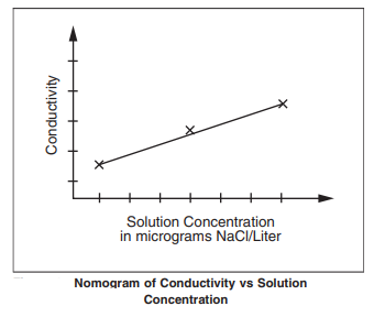
The conductivity of a sample is dependent on the number of ionic materials present. The conductivity of the solution increases as the ionic contamination increases. Also, there are two different types of impurities present on the PCB sample i.e., ionic and non-ionic. Ionic impurities are typically flux residues or chemicals that are accumulated during the manufacturing processes.
Water-soluble organic and inorganic salts may also be present on the PCB sample. These water-soluble organic and inorganic salts consist of charged atoms that are conductive in nature. The charged (positively or negatively) molecules increase the overall conductivity of the solution. These ionic impurities present on the sample degrades the reliability of the PCB assemblies. The impurity can cause current leakage, thus leading to dendrite growth. This will further lead to corrosion of the PCB. Different types of impurities include sodium formate, chloride, bromide, nitrate, and sulfate. The impurities are calculated in mg/em2.
As per the IPC 650 2.3.28, the surface area of the sample is calculated by the formula:
(Length x Width x 2) + 10% for a populated PCB with 75/25 IPA/H20 solutions
The addition of 100-250 ml of the extraction solution to the extraction bag is recommended.
Benefits of cleanliness measurement for ionic contamination
The PCB sample dipped in an extraction solution releases ions with an extraction liquid, which is determined by a conductance detector. The final result is calculated by an ionic contamination meter with the help of software. The measurement value is analyzed with reference to sodium chloride. The resistivity/conductivity readings can be used to convert the µg NaCl equivalent as follows:
Benefits:
- The cleanliness measurement is ideal for post soldering evaluation as per official regulation. Also, it verifies surface quality prior to PCB coating and other chemical processes.
- The testing also performs quantitative determination of the ion contaminates for PCBs in µg/cm² equivalent NaCl.
- The cleanliness measurement continuously monitors contamination of quality through regular sample-based measurement.
Also read, what is conformal coating?
PCB cleaning process
PCB cleaning is a delicate process, similar to manufacturing. A number of issues may arise leading to ionic contamination including, damaged and loosened connections, and washed away materials if the cleaning process is not performed properly. Here are a few PCB cleaning processes worth mentioning:
- Aqueous cleaning process
- Semi-aqueous process
- Vacuum cleaning process
- Vapour phase degreaser
The use of ultrasonic cleaning machines for PCB cleaning has increased over the past few years. The ultrasonic cleaning offers cavitation at high frequencies with the implosion of billions of bubbles in the cleaning solution. The process blasts away contaminants present on the PCB placed in the ultrasonic tank.
Sierra Circuits loves cleanliness, whether it’s in our office, our manufacturing floor, and even our PCBs. Learn more about our PCB assembly steps.
Ionic contamination analysis is introduced to examine the cleaning efficiency and stability of a cleaning process where aggressive chemistry (etching liquid, hot air leveling flux, and electrolytic solution) is being used. Ionic contamination generated by PCB materials and processes can speed-up the electrochemical processes under high-temperature and high-humidity conditions. PCB ionic contamination analysis is performed to determine which method of cleaning would be suitable for the board.

Design for Manufacturing Handbook
11 Chapters - 96 Pages - 90 Minute ReadWhat's Inside:
- Annular rings: avoid drill breakouts
- Vias: optimize your design
- Trace width and space: follow the best practices
- Solder mask and silkscreen: get the must-knows
Download Now