


Contents

On-demand webinar
How Good is My Shield? An Introduction to Transfer Impedance and Shielding Effectiveness
by Karen Burnham
The flying probe test (FPT) is an inspection method that verifies the electrical integrity of a circuit board, especially in low-volume prototypes. As a PCB designer, understanding the process helps you place test points efficiently, enabling faster and more reliable testing.
Highlights:
- Flying probe testing is a fixtureless alternative to ICT (in-circuit test), ideal for low- to mid-volume and prototype PCB assemblies.
- FPT can test for opens, shorts, resistance, capacitance, polarity errors, micro-shorts, and phase differences.
- Key components of FPT systems include probes, test fixtures, and control software for program generation, probe path optimization, and data analysis.
- FPT offers better test coverage, flexibility for design changes, and cost-effectiveness for small batches.
In this article, you’ll learn the steps involved in FPT and practical guidelines for designing test points that ensure accurate electrical validation.
Why is ICT not ideal for low-volume PCB production?
ICT requires a custom, time-consuming, and expensive bed-of-nails fixture, making it inefficient and uneconomical for small batch or prototype builds.
In-circuit test is a form of white-box testing used to verify the functionality of a fully assembled printed board. It uses electrical probes to check for issues such as shorts, opens, and incorrect values of resistance, capacitance, and other basic electrical parameters.
Traditionally, ICT relies on a “bed of nails” fixture-based system, where a custom fixture is built for each design. This fixture contains spring-loaded pogo pins, each precisely aligned to contact specific test points on the PCB assembly. Each pogo pin probes a single node or test point on the board.
Building a custom ICT fixture for a new PCBA can be both costly and time-consuming, especially for complex boards, where manufacturing the fixture may take several days. Because of this, ICT is best suited for high-volume production runs. For smaller batches or prototype builds, it is neither cost-effective nor efficient.
To address these limitations, manufacturers turn to the flying probe testing method.
What is flying probe testing?
FPT is a type of circuit board test that uses flying probes. These probes move between test points according to instructions defined by software specific to the board under test.
No custom fixture is required, so it could also be called a fixtureless in-circuit test if used on an assembled printed board. Hence, it is highly cost-effective for prototypes and low to mid-volume production.
Watch the full video to learn how FPT is performed at Sierra Circuits.
The table below summarizes what FPTs can check for.
| Test type | What it checks |
|---|---|
| Standard tests | Opens, shorts, and connectivity faults across nets |
| Presence and placement of resistors and capacitors, and some active devices | |
| Component values such as resistance, capacitance, and inductance (RLC) | |
| Polarity errors | |
| Advanced tests | Micro-shorts and high-resistance defects |
| Diode/IC input impedance | |
| Phase difference measurements |
Most FPTs are equipped with cameras for automatic component polarity inspection.
At Sierra Circuits, we use the Seica Spa Pilot V8 for flying probe testing. This advanced system delivers high performance, faster test speeds, and is ideal for low- to medium-volume runs. Its simultaneous vertical probing on both sides of the PCB accelerates debugging and provides greater flexibility for prototyping.

It can handle boards up to 600 × 540 mm in size and components up to 40 mm high on both sides. Flying probe testing requires ODB++ files.
Visit flying probe testing for PCB assembly to learn more.
What are the components of FPT systems?
A flying probe tester relies on three core components: probes, test fixtures, and control software.

Let’s see each of them in detail:
- Probes: They are the contact points between the tester and the board. They transmit signals for measurement and analysis, moving in x, y, and z directions to access pads and vias. Common types include:
- Spring-loaded probes (pogo pins): Cost-effective and reliable for general testing.
- Active probes: Equipped with built-in electronics for high-frequency or sensitive measurements.
- Kelvin probes: Four-wire probes for precise low-resistance testing.
- Test fixtures: Fixtures hold the PCB securely during testing, ensuring accurate probe contact and preventing false readings or damage. Types include:
- Mechanical (universal) fixtures: The most common fixture type, built with a rigid frame, clamps, and support pins. Simple and cost-effective, but requires manual adjustment.
- Control software: The software coordinates probe movement, fixture control, and data processing. Its core functions are:
- Test program generation from ODB, IPC-2581.
- Probe path optimization to speed up testing.
- Data analysis and reporting with pass/fail results and SPC charts.
- System integration with AOI, X-ray, or pick-and-place machines.
- User interface and debugging tools for real-time monitoring, error logging, and test refinement.
6 benefits of flying probe testing
- Cost-effective for small lots: FPT is more economical than ICT for prototypes and low-volume production runs.
- Better accessibility: Unlike ICT pogo pins, flying probes can reach much smaller pads and component pins without requiring dedicated test points.
- Flexible test strategies: Probe movement is software-controlled, making it easy to update programs or adjust probe landing positions without hardware changes.
- Improved test coverage: Probes can access component pins directly, enabling broader coverage compared to ICT.
- Non-destructive testing: Gentle probe contact minimizes the risk of damaging thin PCBs or sensitive components.
- Scalability and future-ready: Systems can be upgraded with more probes or software features to support higher volumes and more complex designs.
ICT vs. FPT
| Criteria | In-circuit testing (ICT) | Flying probe testing (FPT) |
|---|---|---|
| Best suited for | High-volume | Low-volume and prototypes |
| Fixture requirements | Requires a custom bed-of-nails fixture | No custom fixture needed |
| Programming | Longer programming time due to fixture creation | Faster programming using CAD data |
| Per-unit cost | Low (once the fixture is made) | High (longer test cycle time) |
| Test cycle time per PCB | ~1 minute | Up to 15 minutes |
| Coverage | Shorts, opens, resistance, capacitance, component tolerance, logic functionality, LED verification, FPGA on-board checks, BTC solder pressure tests | Shorts, opens, resistance, capacitance, component tolerance, LED verification, FPGA on-board checks |
| Connector and non-electrical component testing | No | No |
| Development lead time | Long | Short |
| Adaptability to design changes | Low (requires a new fixture for major changes) | High (changes implemented via reprogramming) |
| Cost | High up-front cost (fixture + programming), but low per-unit cost once the fixture is made | Low up-front cost (programming only) but higher per-unit cost due to longer test cycle time |
To learn how to include reliable test points in your layout, download the Design for Testing Handbook.

Design for Testing Handbook
7 Chapters - 28 Pages - 45 Minute ReadWhat's Inside:
- PCB testing strategies
- Guidelines to design and place a test point for FPT
- Directives to make your board ICT compatible
- Benefits and drawbacks of various testing methods
- Defects that you can identify through board testing
Download Now
How does flying probe testing work?
FPT generates a test program based on the design data, and the probes contact the test points to measure the electrical parameters. The system analyzes the results to verify component values and circuit performance.
Here are the steps your assembly house follows to test a printed board using FPT:
Step 1: Creating the test program
Every FPT provides a test program generating application that runs on a PC.
It requires two key inputs:
- Bill of materials in Excel format.
- Intelligent CAD production files (ODB++ or IPC-2581).
Once the test program is generated, it is loaded into the tester. The circuit board assembly to be tested, which could be either a single board or an array of boards, is placed on a conveyor system, which carries it into the tester area where the probes are located.

Step 2: Running the test
When the test program is run, the probes, controlled by the program, make contact with:
- Component pads
- Test pads (if available)
- Unmasked vias
The tester then applies electrical test signals and power to these probe points and records the measurements.
Step 3. Processing the results
The tester processes these measurements to determine whether the probed circuit section performs as expected, based on the components present, and within the specified tolerances.
To accomplish this, FPT hardware includes:
- Signal generators
- DC and AC power supplies
- Various sensors
- Multiplexing systems
- Digital multimeters
- Frequency counters
These instruments provide excitation signals to PCB nodes and capture measurements from components and interconnections.
Through a virtual isolation technique, the tester uses excitation signals to separate, as far as feasible, the component segments between probes from the rest of the circuitry. This allows component values to be measured as accurately as possible without physically removing them from the circuit.
FPT tries to test the board as comprehensively as possible, given the accessibility constraints of a given board design. To learn about design basics, read, mastering the art of PCB design basics.
Comparison of FPT system types
Flying probe test systems come in several configurations, each tailored to specific PCB testing needs. The choice of system depends on factors such as board complexity, production volume, available floor space, and budget.
The table below summarizes the main types of flying probe test systems, outlining their features, advantages, limitations, and ideal use cases.
| Type | Description | Advantages | Limitations | Use cases |
|---|---|---|---|---|
| Single-sided | Probes access only one side of the printed board at a time. |
|
|
|
| Double-sided | Probes can access both sides of the board simultaneously. |
|
|
|
| Vertical | Tests the board in an upright (vertical) position, with probes configured for single- or double-sided access depending on the tester model. |
|
|
|
| High-speed | Optimized systems using advanced motion control and precision probes to reduce test cycle time. |
|
|
|
Explore why PCB quality standards and inspections are essential for performance and long-term durability.
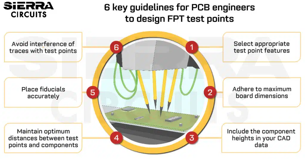
6 key guidelines for PCB engineers to design FPT test points
To ensure reliable and accurate flying probe testing, PCB designers must carefully plan test point placement. The following six guidelines provide actionable recommendations to optimize boards for FPT.
1. Select appropriate test point features and sizes
Choose test points that facilitate reliable contact with FPT probes.
- Select contact points that are most suitable for FPT, such as:
- Test pads without solder resist
- Vias
- Through-holes
- PTH and SMD component pads
- Set the dimensions and spacing of each test point to ensure consistent probe contact.
- The minimum size is 6 mil (20 mil recommended). The size also depends on the probe type. Always check with your assembly house and get their recommendations.
- The spacing between one test point to another should be a minimum of 10 mil to 20 mil.
- Ensure vias are suitable for probe contact.
- The diameter should be between 8 to 20 mil (10 mil recommended).
- Vias must be free from the solder resist.
- Ask your manufacturer to extend solder pads for small SMD components. For SMD pads smaller than 25 mil, use a solder pad longer than the component pin. This allows the probe to contact the pad itself rather than the pin, improving test reliability. Mention this requirement in your PCB fab notes.
2. Adhere to maximum board dimensions
Ensure that the board fits within the tester’s specifications:
- Pilot L4: Maximum 600 × 1010 mm
- Pilot V8: Maximum 600 × 540 mm
Boards exceeding these dimensions may not fit securely or may interfere with probe movement. Always check with your assembly house before finalizing the board dimensions.
3. Include the component heights in your CAD data
Mention the component heights in the CAD data to ensure the board remains compatible with the tester.
Check with your manufacturer to confirm the type of flying probe tester they use and ensure that the component heights in your CAD data comply with the tester’s specifications.
| Tester type | Board side | Maximum height (board + components) |
|---|---|---|
| Horizontal Pilot L4 | Top (head) side | 40 mm |
| Horizontal Pilot L4 | Bottom side | 100 mm |
| Vertical Pilot V8 | Either side | 40 mm |
Provide a list of components whose height is over 17 mm to avoid interference with probes.
4. Maintain optimum distances between test points and components
Clearance is critical to prevent probe misalignment or shorting. Use the formula:
L = (0.29 x component height in mm) + 0.7 mm
This estimates the minimum distance between the center of a test point and adjacent components.
5. Place fiducials accurately for reliable alignment
To ensure precise probe alignment during testing, place fiducials accurately on the PCB. For optimal placement, follow these key recommendations:
- Include 2 fiducials for each board.
- Position the fiducials on either side of the board. It is essential to achieve different arrangements of the fiducials to eliminate side errors.

2 fiducial markers placed on the board for alignment. - For the larger boards with dimensions greater than 400 mm, place local fiducials concerning the fine-pitch components, which must be visible after the component has been mounted.
6. Avoid interference of traces with test points
Route traces carefully to prevent collisions with probe points. Avoid wiring that obstructs pads or vias designated for FPT probing. Proper trace clearance ensures consistent test coverage and reduces the risk of measurement errors.
For DFA tips, download the Design for Assembly Handbook.

PCB Design for Assembly Handbook
6 Chapters - 50 Pages - 70 Minute ReadWhat's Inside:
- Recommended layout for components
- Common PCB assembly defects
- Factors that impact the cost of the PCB assembly, including:
- Component packages
- Board assembly volumes
Download Now
3 emerging advanced features in flying probe testers
Modern flying probe testers now incorporate three advanced capabilities: phase difference measurement, high-voltage stress testing, and micro-short detection.
1. Phase difference measurement unit
The phase difference measurement unit (PDM) injects a high-frequency signal between a reference line and a section of the signal line. It then measures the signal’s phase shift at the opposite endpoint, estimating the phase difference. This method helps reduce the need for conventional isolation tests within a net.
2. High voltage stress test
The high voltage stress test (HVS) is designed to detect high-resistance isolation defects that may go undetected by PDM. HVS applies high-voltage pulses between signal lines to reveal such defects. Both PDM and HVS share the advantage of inspecting each net only once, making them rapid in execution.
3. Micro shorts detection
The sudden application of a high voltage in isolation tests may cause the burning out of parts containing micro shorts. Micro short tests can avoid such damage by gradually increasing the applied voltage from a lower starting point.
In some cases, high-resistance shorts buried between multiple board layers behave like semiconductor junctions or capacitors. By reversing the polarity of the applied high voltage, these hidden defects can also be revealed.
Key takeaways:
- ICT uses custom bed-of-nails fixtures with pogo pins to test assembled boards, making it ideal for high-volume production but costly and time-consuming for prototypes.
- Flying probe testing provides a fixtureless alternative, moving probes between test points under software control, making it highly cost-effective for low- to mid-volume and prototype boards.
- Essential flying probe test point guidelines for PCB designers cover net accessibility, test point selection and sizing, component positioning, board clamping, maximum dimensions, minimum clearances, fiducial placement, and trace routing.
- FPT programs are created offline using CAD/ECAD files and BOM data, then executed on the tester with probes contacting pads, test points, and vias.
Flying probe testing has become a preferred, cost-effective solution for low-volume and prototype PCB assemblies. Ongoing technological advances are enhancing test coverage, improving quality, and shortening testing time, making FPT a powerful tool for reducing product design cycles and accelerating time to market.
Need assistance in designing your PCBs? Post your queries on our forum, SierraConnect, and our experts will answer them.

About Pooja Mitra : Pooja Mitra is an electronics and communication engineer. With an experience of over three years in the PCB industry, she creates industry-focused articles that help electrical and PCB layout engineers.


Start the discussion at sierraconnect.protoexpress.com