Contents

On-demand webinar
How Good is My Shield? An Introduction to Transfer Impedance and Shielding Effectiveness
by Karen Burnham
The cross-section or micro-section analysis is a destructive analysis that measures the quality of the manufactured board. It’s basically an interconnection defect analysis process that detects and verifies what went wrong inside the PCB. This is an integral part of the PCB manufacturing process.
In other words, it’s a process of inspecting the internal quality of a PCB. The inspection is carried out to determine the quality of the circuit board and also to spot internal failures.
In simple terms, it’s like a physician taking a biopsy just to check if the patient is suffering from some kind of disease.
Aspects to consider before the analysis
It is of critical importance to analyze the quality of the boards being fabricated during the PCB manufacturing process.
What is a test coupon?
An efficient way to analyze board quality would be to fabricate additional extensions of the boards being manufactured called PCB Test Coupons. These board extensions will have the same specifications (trace width, copper weight, via structure, etc.) as the original PCB. These coupons will then be tested to recognize material, manufacturing, and other defects.
The test coupons placed at almost every end of the board are cut out close to 1inch square. These coupons are placed in a soft molten polymer that solidifies right around the sample PCB.
The sample board enveloped with the polymer is called a puck. This is because the sample PCB placed at the center looks like a hockey puck. The hardened specimen is finely ground and polished to form a smooth surface finish. This process is carefully done such that the internal parts of the PCB are exposed for observation.
This cross-section i.e. the exposed interior region of the PCB is magnified and examined under a microscope by an expert.
Sample observation
The sample is observed in the As-polished condition (recommended) and As-etched condition.
As-polished
Here the sample is visually inspected right after the sample polishing process.
As-etched
After the polishing process, the sample is etched and visually inspected to find anomalies. Also, here you can observe the component lead grain structure and plated copper grain structure. Under the magnified view, the observer can clearly see the grains of the hole wall and the knee region.
Inspection criteria and the test coupons
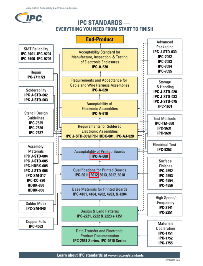
The criteria for inspection are specified by the customer (IPC 6012). Also, the coupon design should follow IPC’s 2220 standard.
The test coupons are placed along with the board panels and go through the whole process that the desired PCB goes through. The main intention of using test coupons is to perform the tests and verify the quality of the board without destructing the desired PCB.
It must be noted that different coupons are used for different kinds of tests. The same coupon cannot be used to verify other parameters since it is a destructive test procedure. Read how we manufacture controlled impedance PCBs.
Through hole coupons:
- Used to determine surface plating and hole wall plating thickness
- Separation of inner layers
- Registration of the drill to the outer and inner layer images
- Inner layer connectivity
- Condition of the laminated materials around a hole
The coupons are also used to evaluate:
- Solderability
- Peel strength
- Electrical characteristics of inner layer traces
- Solder mask
- Legend inks
Assessments
- PTH assessments
- Via assessments
- Hole (barrel) wall quality
- To view the hole Barrel structure
- Quality of the copper plating and plating thickness
- Voids
Refer to our post on lamination voids and delamination in PCB manufacturing to understand more about voids and their effects.
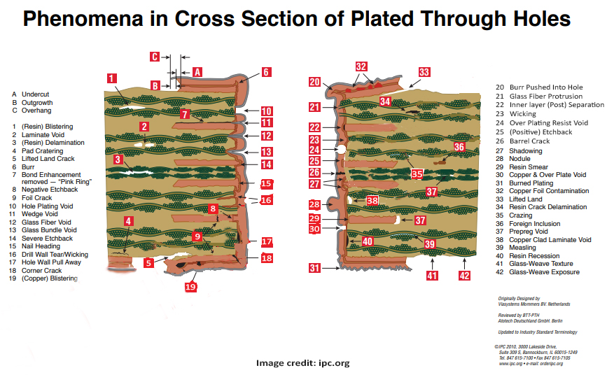
There are two kinds of cross-section samples considered:
- A vertical cross-section (along the PTHs for observing the barrel wall)
- Horizontal cross-sections (Plan View) are used to observe the via and the annular rings. Some of the defects can be spotted only with the horizontal view making it an important perspective in the analysis.
Read PCB quality to ensure compliance with industry-standard testing and fabrication best practices.
Cross-section analysis sample preparation
Sample preparation before cross-section
The coupons are coded depending on their location in the panel. They will be labeled as Left Bottom Coupon (LBC), Right Top Coupon (RTC), and Horizontal Coupon (HC). This will help recognize which panel they belong to and will assist in sorting the poor product from the rest.
The labeled coupons are separated from the board using a low-speed diamond saw with a coolant. These coupons are washed in an ultrasonic cleaning system and Deionized (DI) water.
Sample preparation for standard vias and filled vias (Before cross-section)
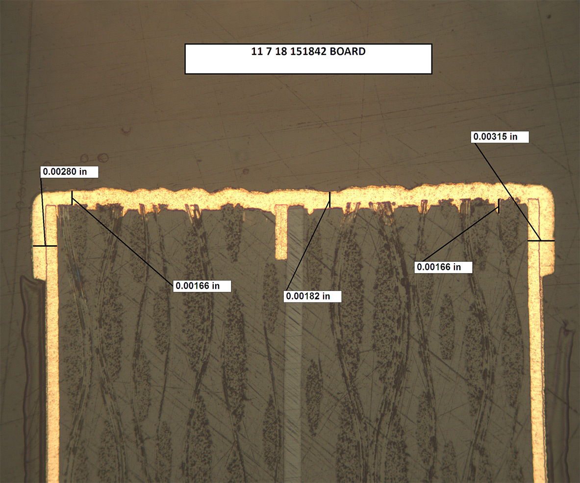
After the sample preparation process, the coded coupons are subjected to cross-section. The initial samples are micro-etched before digital photography. The digital photographs of each of the samples will be recorded. If the samples exhibit defects then this region is magnified to 100X and photographed. The photographs are provided separately.
The detailed measurements are recorded for parameters like:
- Start (Basic) copper thickness
- Copper plating thickness
- Etch back dimensions
- Total copper thickness
- Solder plating thickness
- Dielectric thickness

Design for Manufacturing Handbook
11 Chapters - 96 Pages - 90 Minute ReadWhat's Inside:
- Annular rings: avoid drill breakouts
- Vias: optimize your design
- Trace width and space: follow the best practices
- Solder mask and silkscreen: get the must-knows
Download Now
Sample preparation three or six times solder dipped (Before cross-section)
Here, as per the job request, the particular specimen is subjected to three- or six-times solder dip test before micro sectioning. Like the previous process, even here the observed faults are magnified to 100X. These photographs are provided separately with the report.
The procedure is as follows:
- The specimen is isolated using a diamond saw and the edges are smoothened.
- The sample is washed with Isopropyl Alcohol (IPA) and dried.
- Later, this specimen is baked at 125°C for a duration of 10 hours with an air circulating oven.
- No moisture content should be present before the specimen is subjected to solder bath. The presence of moisture content is hazardous.
- The solder bath process is started by setting up the temperature to 288°C.
- When the required temperature is achieved, the flux applied and the sample is attached to the sample holder.
- The sample is dipped in the molten solder for precisely 10 seconds
- The sample is allowed to cool off.
- The dip process is repeated 3 times or 6 times as per the request.
- The surface is carefully inspected and the defects are spotted.
- Cross-section of the sample is conducted.
- Digital photographs are taken and filed with the report.
- If defects are observed then 100X magnified images are taken which are provided separately.
- The complete report is prepared at the end.
Rework simulation sample process (Before cross-section)
In this process a particular specimen is assigned for rework simulation test:
- The specimen is isolated using a precision diamond saw and the edges are ground.
- This sample is cleaned with Isopropyl Alcohol (IPA) and dried.
- The interconnection resistance is measured from the beginning of the square pad (daisy chain) to the end of the square pad.
- At 260°C, soldering and re-soldering of wire are performed four times. On the fifth time, the wire is soldered and left for examination.
- The sample is washed with Deionized (DI) water and dried.
- Now, the interconnection resistance is measured once again from the beginning of the square pad to the end of the square pad.
- The interconnection resistance measured after rework simulation shouldn’t be above 10% of the initial readings.
- The cross-section of the sample is performed.
- The reports are prepared.
Peel strength of tracks
The peel strength test is conducted only on 3mm conductor width through these steps:
- The sample is isolated and the edges are smoothened.
- The specimen is washed with IPA and dried.
- The conductor width is measured using a profile projector and is noted down.
- The machine is validated with standard weights.
- The selected conductor is peeled back at one end for a length of about 10mm.
- The detached end of the conductor is firmly gripped over its whole width.
- The traction is applied in a direction perpendicular to the plane of the PCB until the copper starts to peel off. The rate of traction is kept at 50mm/min.
- The traction direction is kept perpendicular to the plane of the PCB.
- The force gauge utilized will have a minimum resolution of 0.1g.
- The values are recorded in kg/cm units.
IPC Class 3 Design Guide
8 Chapters - 23 Pages - 35 Minute ReadWhat's Inside:
- IPC guidelines for manufacturing defects
- IPC standards for assembly processes
- Common differences between the classes
- IPC documents to set the level of acceptance criteria
Download Now
Microsection/Cross-section sample preparation
The steps mentioned below are followed for the cross-section process:
- The coupon is separated by a diamond saw or a PCB cutting machine.
- The sample is cleaned with IPA and water.
- The sample is coded and stacked.
- The cup cleaning, the preparation, and releasing agent application is performed.
- The resin and hardener are mixed with an appropriate ratio without entrapping air bubbles.
- The epoxy filling of PTHs is conducted without the formation of air pockets.
- The Sample is mounted in the molten epoxy.
- The mold is filled and allowed to solidify.
- The molded sample is coarsely ground using an automatic belt grinder with 80 grit and fine grinder with 240, 320, 400, and 600 grit.
- This sample is further polished with 0.3micron alpha-alumina powder and finely polished with 0.05micron gamma-alumina powder.
- The samples are observed under the microscope and called an “As-polished” sample.
- The cleaned and dried sample is micro-etched for “As-etched” sample analysis.
- After these steps, analysis and digital photography are carried out.
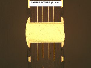
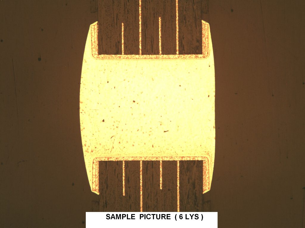
Cross-section analysis process
After the cross-section, the critical aspect, analysis of the sample is conducted.
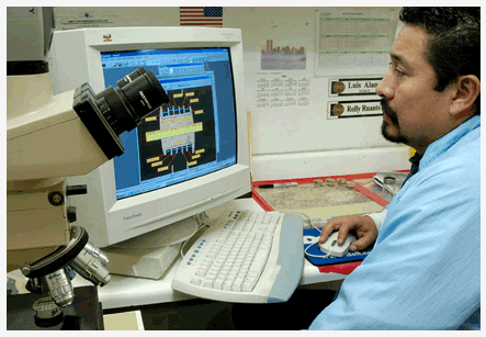
The previously acquired data of the failed samples plays a critical role in the failure analysis process. This data gives an idea and predicts the anomalies that one can expect.
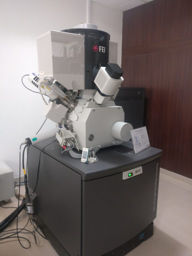
Here, the sample is visually inspected with a Metallurgical and Electron microscope. The parameters observed and recorded are:
- Z-axis expansion
- Barrel cracks
- Pad lift
- Corner cracks
- Uniformity of copper plating inside the barrel
- Voids and uniformity in cap plating
-
Copper:
- Total copper on top and bottom land regions
- Copper deposited on top and bottom land regions
- Basic copper on top and bottom land regions
- Copper deposited in the wall
- Separate inner layer copper thickness
- Copper plating discontinuity
-
Solder thickness at the:
- Center of the top and bottom land regions
- Knee of the hole on top and bottom land regions
- Side on top and bottom land regions
- Center of the hole
- Conductor undercut at the corner, top and, bottom land regions
- Drilling irregularities
- Number of inner layers
- Annular ring
- Etch back/Desmear
- Misregistration of hole
- Protective coating discontinuity
- Resin recession
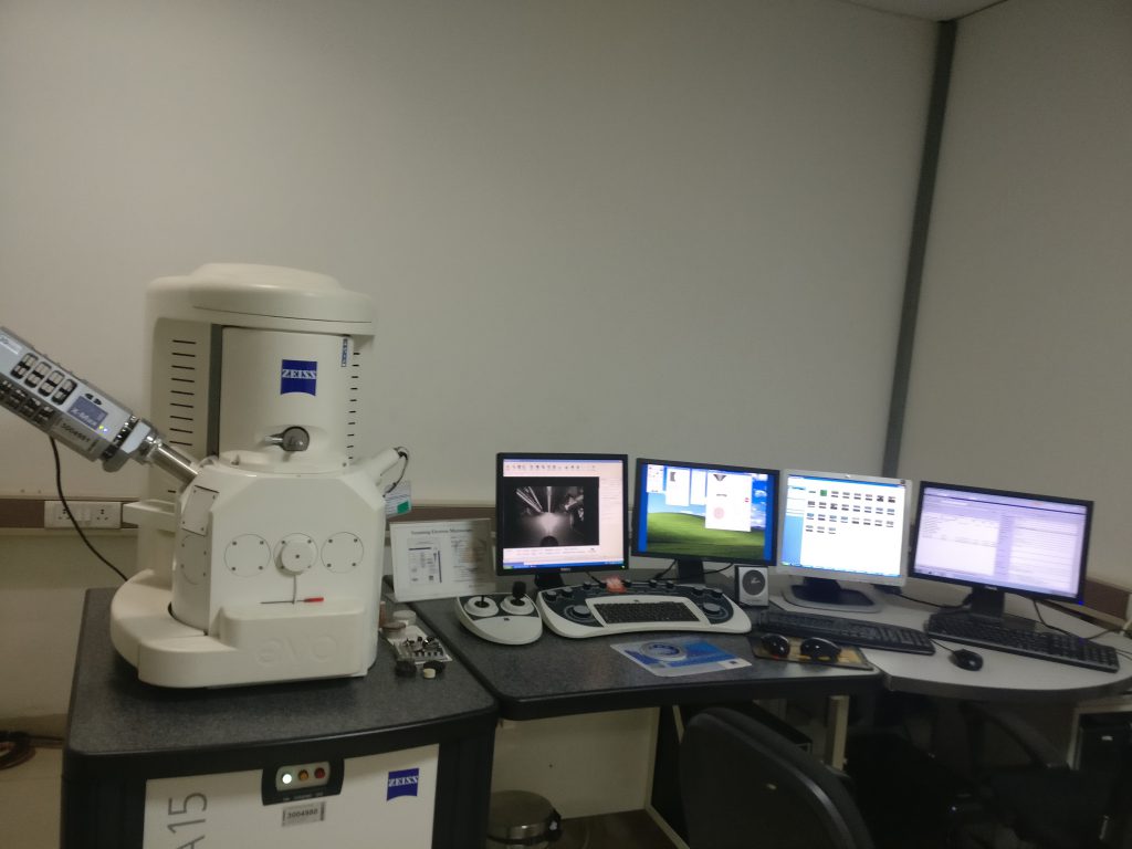
All these observations are recorded and the report with the digital photographs of the parameters is prepared.
The visual inspection will help analyze and identify the faulty internal regions in the PCB. The issues are easily addressed and the quality of the PCB is established. The cross-sectional views of the surface trace work, pads, and solder mask will unravel the unwanted copper, over etch, and poor solder mask and the reasons why a particular part is rejected.
The acquired information from the microsectioning can be used to speculate the errors that could occur during the PCB manufacturing process. This will assist in superior PCB fabrication and help the manufacturers to take the necessary measures while fabricating a printed circuit board.
With the increase in the layer count and decrease in the hole diameter, the implantation of cross-section analysis is becoming crucial. At Sierra Circuits, we have the right infrastructure and experienced staff to perform the extensive cross-section analysis of PCBs.
Also read, what is conformal coating?
See our cross-section lab in the 360 tour of our facilities and email Nagendra at ssdc_nagendrak@protoexpress.com to visit our Sunnyvale, CA-based manufacture and assembly!
About Rahul Shashikanth : Rahul Shashikanth is an electronics and communication engineer with over 8 years of experience in publishing technical articles on PCB design, manufacturing, and assembly. He is currently the content marketing manager at Sierra Circuits.







Start the discussion at sierraconnect.protoexpress.com