


Contents
Today, we are going to talk about signal integrity. As a PCB designer, it is important for you to know the effects of via stubs on signal attenuation and data transfer rates.
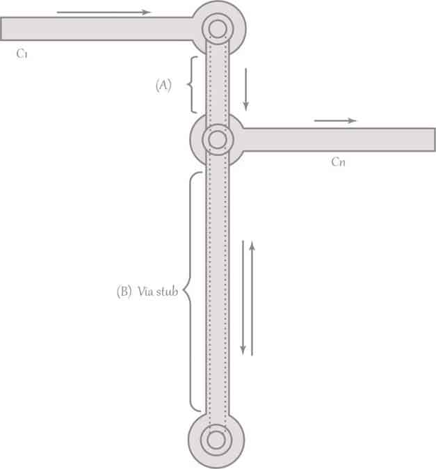
First, let’s start with a few things to know about signal integrity and via stubs. A via stub is the part of a via which is not used for signal transmission. In the example depicted below, the part A of the via is used for signal propagation from the conductor C1 on an outer layer to the conductor Cn on an inner layer. But the part B of the via is extraneous – thus, the via stub in this case.
A via stub acts like a resonant circuit with a specific resonant frequency at which it stores maximum energy within it. If the signal has a significant component at or near that frequency, that component of the signal will be heavily attenuated due to the energy demands of the via stub at its resonant frequency.
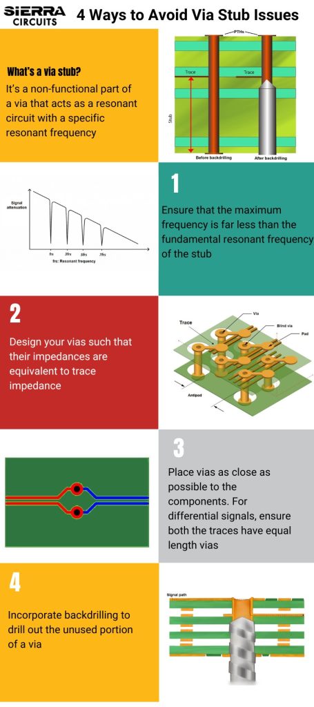
Check out our infographic 4 ways to avoid via stub issues to learn how to eliminate via stubs for optimal signal integrity.

High-Speed PCB Design Guide
8 Chapters - 115 Pages - 150 Minute ReadWhat's Inside:
- Explanations of signal integrity issues
- Understanding transmission lines and controlled impedance
- Selection process of high-speed PCB materials
- High-speed layout guidelines
Download Now
Why does a via stub act like a resonant circuit?
When it comes to signal integrity, you have to know that when the signal travels from C1 to the point of junction between the via and Cn, it splits into two parts – one part travels along Cn and the other part travels along the via stub (B) where it travels to the end of the via stub and is totally reflected back to reach again the point of junction, where it splits again and part of it goes to the destination along the conductor Cn, and the rest goes to the source along the conductor C1.
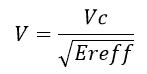
Now, a signal comprises various sinusoidal components of different frequencies and amplitudes as indicated by its spectrum or Fourier’s transform. If ‘f’ is the frequency of a sinusoidal component of the signal, then its velocity ‘V’ in a medium of dielectric constant ‘Ereff’ is given by:
Where:
![]()
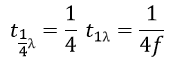
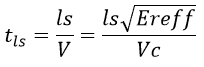
The time period of one wavelength is:

So the time for quarter wavelength is:
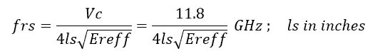
The resonant frequency ‘frs’ of a stub of length ‘ls’ is the frequency of a sinusoidal wave whose quarter wavelength equals the length ‘ls’ of the stub.
Now, the time taken by a signal traveling at speed ‘V’ to travel a length ‘ls’ is given by:
At resonant frequency ‘frs’, as per the definition given above, this time should equal the time taken by a quarter of the wave of frequency ‘frs’:
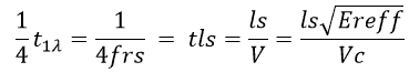
Which gives us the following expression for ‘frs’:
A signal of this frequency will take half wavelength time to come back from the stub to the junction point again and will, therefore, be 180 degrees out of phase with the original signal, thereby considerably attenuating the signal at the junction point.
Thus, the stub acts like a ‘devourer’ for signal energy in a very narrow band around this ‘frs’ frequency – it will store any incoming energy of frequency ‘frs’ in itself and not allow it to propagate further. These are precisely the characteristics of a resonant circuit – and that is why ‘frs’ is called the resonant frequency of the stub.

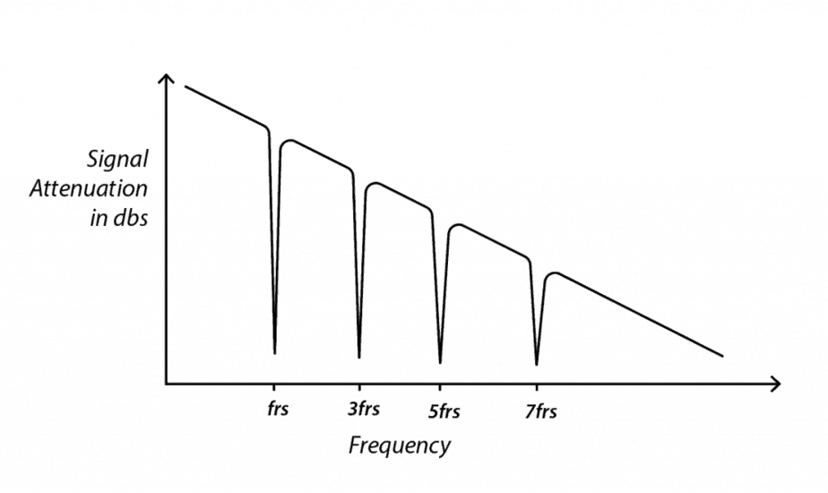
Actually, ‘frs’ is the fundamental (or lowest) resonant frequency of the stub. For signal integrity, recall that it is the frequency at which the stub length equals one-quarter wavelength and total to and fro propagation time equals 1/2 the time period of one wavelength.
The next resonant frequency ‘frs1’ will be such that to and fro propagation time equals (1 + ½ = 3/2) time periods of one wavelength or one direction propagation time over the stub length equals ¾ time period of a wavelength.
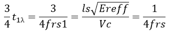
From this, we get: frs1 = 3frs
And similarly, frs2 = 5frs… and so on.
Thus, in the plot of the signal attenuation vs frequency, we will see sharp ‘nulls’ at ‘frs’, ‘3frs’, ‘5frs’… frequencies – basically at the fundamental resonant frequency and its odd harmonics as illustrated below:
Maximum allowable via stub length
If ‘fmax’ is the maximum frequency component of a signal that needs to be faithfully transmitted, then the resonant frequency of the via stub should exceed ‘fmax’ by a good enough margin – a 40% or more margin is sufficient. Therefore:
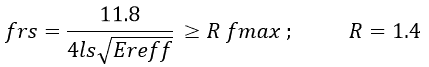
This gives us for ‘ls’:
Value of effective dielectric constant – ‘Ereff’
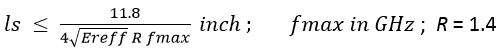
Below is the equation for the maximum allowed stub:
‘Ereff’ denotes the effective dielectric constant of the PCB material. It has been experimentally observed that ‘Ereff’ will be significantly higher than the published ‘Er’ of the PCB material. This is because of two factors:
- Firstly, because of extra via capacitance due to bigger via pads as well as due to close antipads (clearance openings in plane layers). Added capacitance means higher equivalence dielectric constant since capacitance is directly proportional to dielectric constant.
- And secondly, because of the anisotropic nature of the PCB material, the ‘Er’ in (x,y) plane direction being different from ‘Er’ in the ‘Z’ direction. Published ‘Er’ data is usually ‘Er’ in the ‘Z’ direction and it is experimentally found that ‘Er’ in (x,y) direction is ~ 15% to 25% higher than ‘Er’ in the Z direction.
The combined effect of these two factors may make the ‘Ereff’ to be 50% to 60% higher than the published ‘Er’. Therefore, it is prudent to use the following value of ‘Ereff’ in the above calculation:
![]()
Some examples of estimates for digital signals:
For FR-4 material, ‘Er’ ≈ 4.0 ; so ‘Ereff’ ≈ 6.4
For a digital signal of rise time ‘tr’ = 1ns, ‘Fmax’ = 0.5 GHz.
Therefore:
‘ls’ ≤ 11.8/(4x√6.4 x1.4 x 0.5 ) ≈ 1.67 inches, a pretty high value. Since practical PCB thicknesses are much lower than this value, so via stubs in PCBs are of no concern if the fastest signal rise time ‘tr’ is ~ 1ns or ‘Fmax’ is ~ 0.5 GHz.
But for a digital signal of rise time ‘tr’ = 20 ps = 0.02 ns, ‘Fmax’ = 25 GHz. So that:
‘ls’ ≤ 11.8/(4x√6.4 x1.4 x 25 ) ≈ 0.033 inches = 33 mils which is half the thickness of a usual PCB of thickness ~ 62 mils; therefore via stubs are definitely a great concern at this speed of signals.
In fact, it can be readily seen that if ‘tr’ is ≤ 50 ps, or ‘Fmax’ is ≥ 10 GHz, maximum allowable via stub length would be ≤ 0.082 inches, and we would have a via stub problem in case of PCBs of thickness ≥ the maximum allowable via stub length and would have to reduce the stub lengths below the allowable maximum.

And thicker the PCB, greater is the length of the possible via stubs, and, therefore, the lower is the highest signal frequency threshold for the via stub problem to start occurring.
A typical example of this are the digital communication backplanes which are used extensively in Datacom equipment for carrying high-speed digital channel signals from one equipment to another. Such backplane PCBs, being of > 12 layers, are of thickness greater than 0.063 inches – and, often the thickness going up to as much as 0.250 inches. A stub length – ‘ls’ – of 0.250 inches to be tolerable means that ‘Fmax’ needs to be < 3.3 GHz or fastest pulse rise time ‘tr’ needs to be > 150ps or the Data Baud Rate needs to be < 1GBdps, which is pretty restrictive. Hence, in backplanes, via stub lengths need to be controlled.

Signal Integrity eBook
6 Chapters - 53 Pages - 60 Minute ReadWhat's Inside:
- Impedance discontinuities
- Crosstalk
- Reflections, ringing, overshoot and undershoot
- Via stubs
Download Now
Fmax, Baud Rate and Data Rate of a digital channel
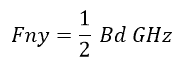
Signals propagating on a digital channel comprise of a series of digital pulses encoded by some definite scheme (like NRZ or PAM-4, etc.) so as to carry the binary digits (bits) information of the signal. This means that the digital signal comprises a series of symbols, each of a definite width in the time domain; the symbols could be changes in voltage levels (one voltage level indicating the bit value ‘0’ and one voltage level indicating the bit value ‘1’) or changes in frequency or phase. A digital signal is thus characterized by a symbols rate – the maximum number of symbol changes per second, which determines the data transfer rate across the channel. The symbols rate is called the Baud Rate (Bd) of the channel. It equals twice the fundamental frequency component of the signal. Baud Rate is usually specified in units of gigabauds per second, or abbreviated as GBdps. The fundamental frequency is also called the Nyquist Frequency of the signal.
If the Baud Rate of a digital channel is Bd GBdps, then:
Nyquist Frequency represents the fundamental frequency in the signal. Usually, the physical channel’s bandwidth (BW) should be at least five times the Nyquist Frequency so that the fifth harmonic of the fundamental is also transmitted by the channel in order to reconstruct the signal faithfully. Thus, the maximum frequency ‘fmax’ of the signal is given by:
![]()
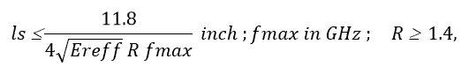
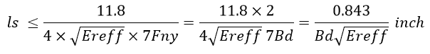
In order to transmit the signal faithfully in the presence of a via stub, we require that the stub’s first resonant frequency should be greater than the fifth harmonic. It is a good rule that the first resonant frequency should be equal to or greater than the seventh harmonic. So the stub length should not exceed the following:
Therefore, if we know the Baud Rate of a digital channel, we can estimate the maximum allowable stub length.

Some digital signaling examples:
NRZ signaling uses two symbols indicated by two voltage levels – LOW and HIGH. As there are two symbols, each symbol represents one bit of data. This is generally the case for most digital signals. Therefore, the Baud Rate is the same as Bit Rate or the Data Rate: Br = Bd; for NRZ signaling.
PAM-4 signaling uses four symbols indicated by four voltage levels. Each symbol thereby indicates 2 bits of data. Therefore, the Bit (or Data) Rate is twice the Baud Rate: Br = 2Bd; for PAM-4 signaling.
In PAM-4, for the same Baud Rate, we thus achieve double the data rate of NRZ case. However, since there are now one of four symbols – voltage levels – to be recognized during a symbol time (instead of the usual ‘one of two’ voltage levels in NRZ), the noise margin available for each symbol level is decreased considerably. While in NRZ there is only one step in voltage level (L to H) to be detected, in PAM-4 there are three voltage level steps to be detected as illustrated below:
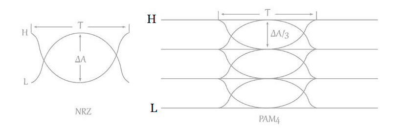
Where:
Delta A = Amplitude step between H and L voltage levels.
Thus the step amplitude, and thereby the signal to noise ratio (SNR) in PAM-4 is one third that of NRZ.
Some examples of maximum stub length estimates for digital channels:
For FR-4 material, Er ≈ 4.0 ; so Ereff ≈ 6.4 √Ereff = 2.53
For NRZ @ 10GBps, Bd = 10 Bdps; thus ls ≤ 0.843/(2.53×10) = 0.033 inches. As the usual thickness of a PCB is 0.063 inches, a via stub could be longer than 0.033 inches. Therefore via stubs should definitely be reduced in length below 0.033 inches.
For NRZ @ 28GBps or PAM-4 @ 56Gbps, Bd = 28 Bdps; thus: ls ≤ 0.843/(2.53×28) = 0.012 inches. Thus almost any via stub is a problem. Therefore via stubs should definitely be reduced in length below 0.012 inches.
Now that you know everything about signal integrity and via stubs, you can read our PCB Transmission Line series and or take our Signal Integrity Quiz. Also, try our PCB Via Quiz
For more information on design rules, check with our DESIGN SERVICE team.

PCB Transmission Line eBook
5 Chapters - 20 Pages - 25 Minute ReadWhat's Inside:
- What is a PCB transmission line
- Signal speed and propagation delay
- Critical length, controlled impedance and rise/fall time
- Analyzing a PCB transmission line
Download Now
About the author: Atar Mittal is the Director and General Manager of design and assembly division at Sierra Circuits. He is responsible for the design and development of strategies and process automation tools for complex printed circuit boards and assemblies. Atar is also currently engaged in the development of productivity tools for electronics designers that would have a tremendous impact on shortening the development time.
About Atar Mittal : Atar Mittal is the General Manager and Director of the Design and Assembly Sierra Circuits division. He has a degree in Electrical Engineering from IIT Kharagpur and has worked in the electronics industry for over three decades.


