Contents
Surface mount technology (SMT) is not a zero-defect soldering process. In this article, we will look into simple defects in surface mount technology that cause your board to fail and try to work out how to avoid them. Reducing such defects is the key to providing efficient PCB assembly services.
Before we go through the errors in SMT assembly, let us go over the basics:
What is surface mount technology?
Surface-mount technology is a process in which electrical components are mounted directly onto the surface of a printed circuit board. An electrical component mounted in this way is called a surface-mount device (SMD).
What are the advantages of surface mount technology?
SMT has several advantages over through-hole mounting. SMT enables ease of automation and higher component densities on the board. It also enables higher circuit speeds while providing better high-frequency performance.
What is the difference between through-hole and surface mount technology?
There are several differences between surface-mounted and through-hole technology. The main differences revolve around cost, automation, board space, and component density. Through-hole components have higher manufacturing costs than SMT components and are not suitable for automation. Through-hole tech also has higher limitations on board space and component density when compared to SMT.

Surface Mount Technology Troubleshooting
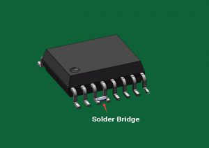
SMT Error #1 Solder-bridging or electrical bridging
Solder bridging is solder across the two conductors that should not be electrically connected, and which cause electrical shorts. These shorts result in a malfunction of the circuit.
Potential causes
- A variety of reasons can account for bridging; however, the most widely recognized reason is an issue in the solder paste printing process. The print arrangement, or stencil arrangement to the PCB pad configuration, can be somewhat off.
- Too much deposition of solder paste can likewise cause bridging. This may happen when the stencil aperture to pad proportion is excessively high.
- Solder paste cold slump can likewise prompt bridging.
- An incorrect solder paste metal-to-flux weight proportion causes a slump. High temperatures and moistness can likewise prompt solder paste slump.
- The reflow profile may likewise add to bridging. We know the purpose of the reflow process is to melt the powder particles in the solder paste. Along with that, it wets the surfaces being joined together and finally solidifies the solder to form a strong metallurgical bond. The profile can be broken down into four zones – the preheat, soak, reflow, and cool-down zones.
- If the pre-heat area has an excessively slow ramp rate, it can account for bridging. Part contact with the solder paste may skew the deposit, making the solder paste bridge. The extended soak will input more heat to the paste and result in the paste’s hot slump phenomenon.
- Placement inaccuracy can further narrow the gap between pads, hence escalating the chance of bridging. Too much component placement pressure can squeeze paste out of pads.
Possible solutions
- Requires an appropriate solder paste metal-to-flux weight ratio. In other words, no slumping of the solder paste. For example, usually dispensable solder paste has a metal content of 85-87% metal. This ratio would slump if we use this for a fine pitch surface mount printing. Typically, 90% metal is, or at least should be, used for a stencil printing solder paste application.
- A suitable reflow profile is also very important.
- Proper attention should be given to the alignment of stencil apertures to pads unless you are using an automatic printer alignment.
- Ensure on-point pressure and accuracy for component placement.
- Reduce the stencil aperture dimensions by 10%. Otherwise, the thickness of the stencil can also be reduced, which will reduce the amount of solder paste being deposited.

SMT Error #2 Insufficient solder joints or electrical opens
When two electrically connected points become separated, or an area on the PCB that interrupts the intended design of the circuit is termed an electrical open.
Potential causes
- The solder paste printing stage of a surface mount process contributes the most to this defect.
- Insufficient solder on the joint will result in the circuit being open. This can happen if solder paste clogs in the apertures of the stencil.
- Even if the solder volume is adequate, an open can occur if it is not in contact with both the lead and the pad during reflow. This is called component lead coplanarity.
- Opens may also be a consequence of the PCB fabrication process itself.
Possible solutions
- First and foremost, the solution is correcting the aspect ratio. The aspect ratio is defined as the ratio of aperture width to stencil thickness. The solder paste clogging the apertures may be due to the aspect ratio being too small.
- Extreme environmental conditions are a strict no-no in the manufacturing process. Avoid solder paste contamination by controlling the environment.
- An investigation regarding coplanarity is also very important when it comes to solving electrical opens.
- Fabrication must be checked with the PCB supplier.
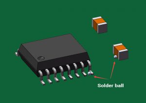
SMT Error #3 Solder balling
It’s the development of very tiny spherical particles of solder isolating from the main body, which forms the joint. This is an essential concern for the no-clean process since an enormous number of solder balls can make a fake bridge between two adjoining leads making functional issues in the electrical circuit. Solder balling isn’t as large a worry with water-soluble procedures since they are regularly removed during the cleaning procedure.
Potential causes
- Moisture contamination of solder paste is one of the major reasons for solder balls. The moisture saturates during reflow leaving solder spheres behind.
- Lack of a proper reflow profile can also lead to solder balls. A fast preheat rate will not provide enough time for the solvent to evaporate gradually.
- Excessive oxides on the solder powder in the solder paste can also form solder balls.
- Solder balling can be caused by poor solder paste printing alignment, as well as when the solder paste is printed on the solder mask instead of the pad.
- Smeared solder paste on the bottom side of the stencil during the printing process is also an attribute.
Possible solutions
- Coarser powder size is recommended as fine powder size has more oxides and tends to slump more readily.
- A reflow process should be selected according to the solder paste.
- Solder paste’s interaction with moisture and humidity should be avoided.
- Check the minimum print pressure used.
- Print alignment should be verified on a consistent basis before proceeding to reflow.
- Ensuring proper and frequent cleaning of the bottom of the stencil.
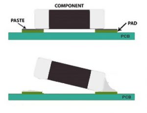
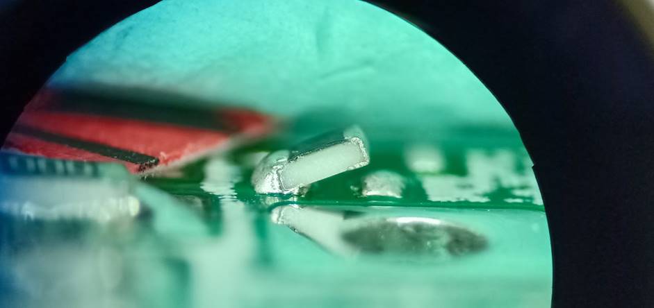
SMT Error #4 Tombstoning
A tombstone, sometimes called the Manhattan effect, is a chip component that has partially or completely pulled off the pad into a vertical position, having only one end soldered. This results from force imbalances during the reflow soldering process. The component stands on one end as if rising from the dead. Therefore, it looks like a tombstone in the graveyard. Actually, it is a defunct PCB design with an open circuit.
Potential causes
- Uneven heating can cause a differential across the component terminals. To be more precise, if the heat distribution is not even, the solder will melt at different rates. Thus, one side reflows before the other, resulting in the other lead standing upright.
- Unequal heat sinks,i.e., ground planes, if present inside PCB layers, may draw heat away from the pad.
- Sometimes, due to temperature and humidity exposure on the solder paste, there is an insufficient force of the solder paste to hold the component in place during reflow.
- Excess movement during and after the reflow operation can cause component misalignment, which results in tombstoning.
- Unequal placement of components on pads prior to reflow results in unbalanced solder forces.
Possible solutions
- The component body must cover at least 50% of both pads to avoid an imbalance in solder forces.
- Ensure a high component placement accuracy.
- It is recommended to maintain a high preheat temperature so that the differential between the two ends is small during reflow.
- Minimizing the movement during the SMT assembly to the least possible during reflow.
- Least exposure to environmental extremes such as high temperature or humidity.
- An extended soak zone can help in balancing the wetting force on both pads before the paste reaches the molten state.

Design for Manufacturing Handbook
11 Chapters - 96 Pages - 90 Minute ReadWhat's Inside:
- Annular rings: avoid drill breakouts
- Vias: optimize your design
- Trace width and space: follow the best practices
- Solder mask and silkscreen: get the must-knows
Download Now
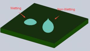
SMT Error #5 Non-wetting or de-wetting
The condition in the solder joint in which the fluid solder has not adhered intimately with at least one of the components. A condition whereby a surface has contacted liquid solder, but has had part or none of the solder holding fast to it.
Potential causes
- Poor PCB finish can be one of the major reasons. Suppose the base metal is visible; typically, this is more difficult to solder to, hence, non-wetting occurs.
- It might also be due to the soaking time being too long in the reflow process. Resulting in exhausting the flux before soldering.
- Possibly during the reflow process, the heat is insufficient, hence, the flux doesn’t get the proper activation temperature.
Possible solutions
- Better quality metal surface finish, such as higher temperature-resistant OSP or ENIG, needs to be adapted.
- Reduction in the total profiling time before the reflow stage.
- Proper flux for the given soldering task.
Also, read how to work around black pad in ENIG finish
SMT Error #6 Solder beading
The formation of bigger solder balls situated close to discrete components having very low distances from each other. This deformity is like solder balling, yet it is discrete in the way that these solder beads hold fast to discrete components rather than multi-leaded gadgets.
Potential causes
- Typically, this kind of problem is due to an excessive amount of solder paste being deposited.
- Sometimes during the preheat stage, there is flux outgassing that can override the paste’s coalescence force.
- Excessive component placement pressure can also be an issue. This can push deposited solder paste onto the solder mask. Hence, not being able to fuse back into the joint.
Possible solutions
- Reducing the stencil thickness or reducing the aperture dimensions. On the side where the solder bead occurs, a reduction of 10% should solve this problem.
- Reducing the component pick and place pressure.
SMT Error #7 Insufficient fills and insufficient solder
The amount of solder paste deposited at the printer station is much less than the stencil opening design or, after reflow, insufficient solder to form a fillet at the component leads.
Potential causes
- The stencil aperture can, at times, get blocked with dried-up paste. This is one of the major causes of the issue.
- During the print cycle, it is of great importance that sufficient pressure is applied across the entire length of the squeegee blade. This will ensure a clean wipe of the stencil. Too much pressure can cause scooping of the paste, especially from larger pads, and this can result in the defect.
- Paste does not roll into the aperture due to too high squeegee speed. The traveling speed of the squeegee determines the available time for the solder paste to roll into the apertures of the stencil and onto the pads of the PCB.
- When the solder paste viscosity and/or metal content is too low.
Possible solutions
- The large opening can be segmented into smaller apertures and checked for too much squeegee pressure.
- The stencil must be cleaned at regular intervals, and the paste should be checked for expiry or dryness. Also, sufficient board support should be ensured.
- Excessive squeegee speed is also undesirable and should be controlled.
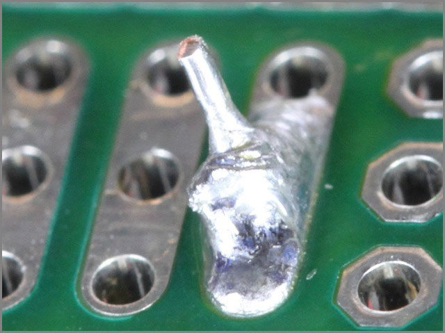
SMT Error #8 Cold solder joint or grainy joint
Some solder connections sometimes exhibit poor wetting and possess a greyish, porous appearance after soldering. It is recognized by dark, non-reflective, rough surfaces of an alloy that should supposedly be bright and shiny.
Potential causes
- One of the major causes listed is insufficient heat absorbed by the solder. This happens because the heat required to reflow the solder is not adequate.
- Many times, during SMT soldering, the flux seems incapable of accomplishing the task. This can be due to insufficient cleaning of the components and/or the PCB pads before they go for soldering. Too many impurities in the solder solution can also lead to a defect.

Possible solutions
- The maximum reflow temperature should be high enough so that the material is reflowed thoroughly.
- The assembly should not experience any sort of movement during or immediately after reflow.
- Alloy analysis must be done to check for contaminants.
With the miniaturization of PCBs, the issues associated with PCB manufacturing are increasing. There is a requirement for tighter control on the solder process with smaller components being used on PCBs. Mitigating common errors in SMT is a major step towards increasing SMT manufacturing efficiency, leading to more effective PCB assembly services.
Quote and order your circuit boards online with our SELF-SERVICE PCB tools in just a few minutes.
Have queries regarding defects in surface mount technology? Post them on our forum, SierraConnect. Our design experts will resolve them.