Contents

On-demand webinar
How Good is My Shield? An Introduction to Transfer Impedance and Shielding Effectiveness
by Karen Burnham
Depending on component technology, many options exist for automated mass soldering today. But wave soldering was the first, and, for several decades, only, practical method for quickly soldering large numbers of components to PCBs because their tracks or traces replaced actual wires previously needed to connect components.
Highlights:
- Wave soldering was the first practical method for mass soldering electronic components onto printed circuit boards.
- Reliable soldering depends on controlling physical forces such as heat, surface tension, wetting, and PCB separation from the solder wave.
- PCB design and component orientation play a critical role in preventing defects like bridging, skips, and incomplete hole fill.
- Advances in electronics, from through-hole assemblies to hybrid and surface-mount designs, have driven continuous evolution in wave soldering technology.
Understanding soldering: From vacuum tubes to miniature solid-state
For the first decade of my life, our home telephone did not have buttons or even a dial. We picked up the receiver and asked a human to make the call. (Our home number was 399J.) Today, my phone is vastly more powerful and flexible than the mainframe computer on which I learned programming.
My first soldering job involved soldering wires to arrays of sockets. Components that looked like incandescent lightbulbs were plugged into the sockets to make things like AM radios. There were a lot of people doing soldering in that factory and, as far as I can remember, no soldering machines.
One of the first units of the solid state mainframe computer (the IBM System/360) that changed the world arrived at my undergraduate university in time for my sophomore year. Commands and data were input with punch cards. Tape reels stored the data. Computer usage was by appointment only (and charged by the minute).
We dropped off our cards and returned at the appointed time to retrieve the printouts from one of the dozens of techs required just to keep the system running. And this was the machine that would change the world!
I bought my first “pocket” calculator in 1972 for $350 (equivalent to a bit more than $2,000 today). It could perform the basic four functions (and nothing more) yet seemed worth every penny of its now absurd cost. My local drugstore was selling more powerful calculators for less than $6 not long ago.
Forty-odd years ago, I worked at a company that made the first word processors. They were the size of a closet, stored data on 10” floppy discs, and cost as much as a Mercedes 450S. About five years later, personal computers not much larger than a mechanical typewriter handled word processing better than the original dedicated machines but cost about 80% less.
Around 1998, an electronics engineering professor of an esteemed university told me in all seriousness that the Pentium 4 processor was so advanced that there would never be applications requiring more power. That chip became obsolete within about 18 months.
In recent years, I have encountered synthetic humans so thoroughly lifelike that they are used for training surgeons. Pocket-size devices are close to performing real-time translation between very different languages. GPS has worked so well for so long that an entire generation has grown up without needing to use a map. And those incandescent lightbulbs that looked a lot like the vacuum tubes that I was soldering 60 years ago disappeared from stores about a decade ago, replaced for the most part by LED electronics.
In my lifetime, then, the world has reached the point where we would have a hard time getting by without electricity and electronics. It only takes a brief failure of the electric grid to prove we are utterly dependent on the movement of electrons.
The transformation in technology has been amazing, and we quite rightly marvel at the remarkable components and assemblies that make this life possible. But the remarkable components are useless without solder, the same material used at least since Edison, to complete the circuit.
Soldering is not as thrilling as new product development, but it’s the very heart of electronics. And, even though we’ve soldered electronics since the 1800’s, the most common problems in electronics still involve getting solder everywhere it’s needed and only where it’s needed without damaging components.
Soldering is often described as an art. And that’s where the problems begin because soldering is all about science. Most soldering problems are easily preventable with an understanding of the physical forces that control solder’s behavior.
Much has been written about solder and soldering by some very smart people who, unfortunately, use complicated terminology and mathematics that can be hard to follow. But we’re here to help.
This is the first in a series of articles intended to take the mystery out of all aspects of soldering, beginning with the first successful method of large-scale production soldering.
You can read Jim Smith’s 8 soldering tips.
Even though it became the most common form of mass soldering before most of us were born and has been in constant use ever since, many people still find wave soldering confusing and hard to manage. So, let’s eliminate the mystery.
What is wave soldering?
It is a manufacturing process used to solder electronic components onto printed circuit boards by passing the board over a wave of molten solder.
The basic principle of wave soldering is fairly simple. After components are placed on the PCB with their leads inserted in holes (“through-holes”) drilled or punched through the circuit board, the assembly is placed on a conveyor. The conveyor moves the assembly across a tank (often called the “pot”) of liquid solder.
The solder is pumped through a chimney to form a ridge that flows across the bottom of the printed board to form connections between the component leads and PCB circuitry. Although the principle is simple, the process requires control of many variables, each of which has the potential to cause serious defects.
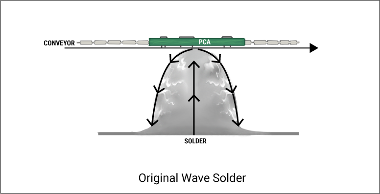
Wave soldering has been used to solder surface mount devices (“SMDs”), but the technology is best suited to “through-hole” assemblies (components with leads inserted in holes drilled through the circuit board).
Download the Design for Manufacturing Handbook for DFM tips.

Design for Manufacturing Handbook
11 Chapters - 96 Pages - 90 Minute ReadWhat's Inside:
- Annular rings: avoid drill breakouts
- Vias: optimize your design
- Trace width and space: follow the best practices
- Solder mask and silkscreen: get the must-knows
Download Now
History of wave soldering
Electronics before the 1950s were not like what we know today. The key components, known as vacuum tubes, looked like incandescent light bulbs but contained electrodes instead of filaments. The tubes were plugged into sockets mounted on a supporting plate. Wires soldered by hand to tabs on the sockets provided the electrical circuitry.
The components and assemblies looked like this:

The arrival of solid-state components and printed circuit boards in the 1950’s dramatically simplified electronics assembly.
The early PCBs were all single-sided (the “printed” circuitry was on one side only).
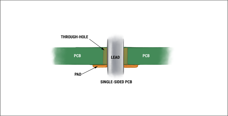
Metal tracks (also known as “traces”) on the laminate replaced the vacuum tube wiring. (For many years, PCBs were commonly known as printed wiring boards or “PWBs” because the circuitry functioned like wires. The “printed” part is less obvious but reflects the method of creating the metal circuitry.
Modern board circuitry starts with copper covering the entire board and removes the unnecessary metal. Originally, however, metal was deposited as a form of lithography used by commercial printers, truly printing the circuitry.) The component leads were inserted in holes drilled or punched through the board and metal. Solder connected the leads to the metal and completed the electrical circuit.
In contrast to the elegant patterns found on modern PCBs, early circuitry was laid out using tape and razor blades, with often ungainly results like this:
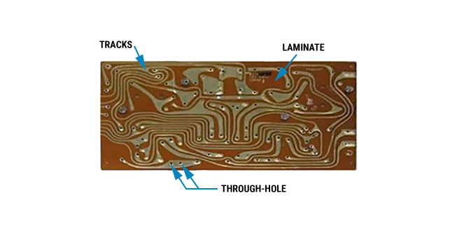
Over time, when the tracks became narrower to allow more circuitry to fit in the same area, donuts of extra metal were left around the through-holes so solder could connect the circuitry to the component lead. These donuts (which, in truth, were not always round) were originally known as “lands,” but gradually “pads” became more widely used.
PCBs would become much more complex over time. Adding metal inside the holes (“plated through-holes”) allowed using both sides of the board for printed circuitry (“double-sided circuit boards”). Laminating boards together (“multilayer PCBs”) allowed the addition of internal tracks.
Pure through-hole assemblies increasingly gave way to “hybrid” assemblies that combined through-hole and SMDs. And some circuit “boards” are flexible ribbons rather than rigid plates. Each new generation of PCBs presented new challenges and requirements for more complex wave soldering machines. But wave soldering began with these simple circuit boards and was just as primitive.
The first printed circuit assemblies were soldered the same way as wired vacuum tube assemblies, by hand. But with all the solder points on a single flat plane, new ways of thinking about process were inevitable. Soldering all the leads simultaneously rather than individually made sense. The question was: how? And the first answer was “dip” soldering.
First effort: Dip soldering
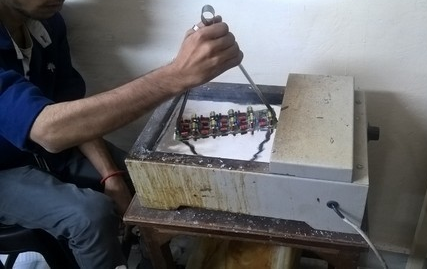
Dip soldering placed the fluxed assembly flat on a pool of liquid solder. And it was not hugely successful. Besides being dirty, hot, smelly, and rather dangerous, the labor savings were modest, and the solder results, opens (no solder), partial connections, webbing, spikes, and shorts, were consistently inconsistent. The process was quickly abandoned except for a few primarily mechanical assemblies.
Second effort: Drag soldering
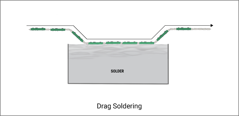
“Drag” soldering (an automated form of dip soldering) came next. Instead of a muscular human to do the heavy work, a conveyor moved the assembly onto, across, and out of a solder pool. This was fairly efficient and much more popular with operators who no longer had to risk burns or inhale fumes.
Third effort: Wave soldering
There were problems, however. In particular, sagging as the hot solder softened the PCB resulted in inconsistent contact (and inconsistent solder connections) between the assembly and the solder bath.
Entrapped flux globs often showed up in connections that should have been filled with solder. (“rosin connection” still shows up in many industry lists of defects, though it probably largely disappeared years ago with the shrinking of solder joints and reductions in the concentration of rosin. Many fluxes no longer even contain rosin.) Solder oxides tended to form webs across the soldered side of the PCB.
And then someone remembered a closely guarded U.S. military secret of WWII. Proximity fuses set off explosives in weapons like bombs when the devices are within range of their targets. America had proximity fuses, and the other side didn’t. The proximity fuses were so effective that authorities regarded them as more important to the war effort than the atomic bomb.

Much of the soldering for fuses had to be carried out by hand. But the connections required for a few subassemblies were all located on a flat surface, which made machine soldering possible. A process of passing these subassemblies over flowing solder was more efficient, practical, and possible. In other words, they used a primitive wave soldering process.
Like the proximity fuses, the manufacturing process was also highly classified until around 1948. It was then declassified with little fanfare and even less interest. In a world of tubes and wiring, there were few applications suited to flow soldering.
The new solid-state circuitry was different. The wires and other items that clustered inside the vacuum tube chassis were gone. All the points to be soldered lay on the same flat surface with nothing to interfere with the solder as it flowed across the bottom of the PCB. Now wave soldering made sense.
To learn how to build reliable boards, download the IPC Class 3 Design Guide.

IPC Class 3 Design Guide
8 Chapters - 23 Pages - 35 Minute ReadWhat's Inside:
- IPC guidelines for manufacturing defects
- IPC standards for assembly processes
- Common differences between the classes
- IPC documents to set the level of acceptance criteria
Download Now
6 key factors that control wave soldering quality
Wave soldering quality depends on the stability of the board contact with the solder wave and proper thermal management. Controlled separation speed and high solder surface tension allow excess solder to drain back into the bath and prevent bridging or spikes. Finally, good wetting (oxide-free metal surfaces) and proper exposed metal area/orientation at wave exit ensure strong joints and reduce defects like bridges and incomplete fill.
To state the obvious, any form of soldering must put sufficient solder everywhere it’s needed, and none where it can cause problems (shorts, balls, spikes, and the like). That’s the minimum requirement.
We would like to go beyond the minimum as much as possible, though. We would like full 360° solder connections without any gaps in the opening between leads and pads. With plated through-holes, the objective should be complete vertical fill of plated holes. While standards mostly allow for less than ideal, understanding and working with the forces that control solder flow makes 100% perfect more likely.
Those forces include:
1. Stable contact between PCB and wave
Complete contact between the solder wave, circuit board, and component leads is essential for proper solder wetting and reliable joints.
2. Heat and thermal management
This has several aspects. First, there must be heat to drive off solvents and activate flux (to deoxidize surfaces to be soldered) before the assembly enters the solder wave. This heat is provided by heaters under the conveyor.
Next, in the simple case of single-sided PCBs (i.e., no plating in through-holes and, therefore, no requirement for solder to flow up the hole), the solder temperature must be high enough that the solder does not freeze before the assembly has separated from the wave.
Finally, for assemblies with plated through-holes, the temperature on the top side of the PCB must be greater than the melting temperature of solder to prevent solder from freezing before achieving complete vertical fill of the hole.
For decades, preheaters were only located under the conveyor. The other source of heat (the solder bath) is also under the conveyor. For heavy PCBs or components with large thermal mass, solder remained liquid long enough to fill through-holes only if the conveyor speed was very slow and/or the solder temperature was higher than necessary.
A longer time over the heating elements could scorch the PCB, while excessive solder temperature generated more dross, degraded machine components faster, and caused sagging or delamination of the printed circuit board.
For almost all modern assemblies, heaters above the assembly as well as below are vital. The greater the amount of energy provided by the top preheaters, the less heat is necessary on the bottom.
Except for components with very heat-sensitive bodies (long ago, bodies made of polyethylene were not uncommon), heating the top of the PCB to 300°F or (occasionally) more before the wave works well. Even with low-melting-temperature components, placing heat shields over the parts typically provides adequate protection.
The term “cold solder” is common in North American electronics. In most cases, the “cold” solder is actually the result of failure to remove oxides (non-wetting, in other words), not lack of heat. (The equivalent term in Britain has always been the more accurate “dry” joint.)
Incomplete vertical fill of a plated hole because the solder froze is the one phenomenon that can properly be called “cold solder.” And the solution is top-side preheaters.
3. Speed of separation of the PCB from the solder wave
Slower separation provides more opportunity for excess solder to drain back into the solder bath.
4. Solder surface tension
Surface tension causes solder to snap back, preventing excess solder, especially bridges. Oxidation of the liquid solder as the assembly leaves the wave reduces the surface tension and causes excess solder. (Solder “icicles” rarely result from inadequate solder heat.
Most “icicles” result from oxides encasing the liquid solder and killing the surface tension that causes the solder to pull back. The “icicle” terminology is erroneous because the spike holds its shape despite the solder being liquid. Without the surface oxide, surface tension would pull the solder back.)
5. Interatomic attraction and wetting
Failure to completely deoxidize leads before they enter the wave results in two defects.
First, solder will not wet to an oxidized surface. Electricity is the flow of electrons from atom to atom in a conductor. Metals in which electrons move most easily are the best electrical conductors. However, those metals do not like being in their pure state with easily moved electrons; they want to combine (i.e., react) with other element(s) to form compounds that lock electrons in place. Where the pure metal had reactive energy, the compound is stable (often referred to as “passive”).
For all practical purposes, solder is pure metal where it contacts a component surface. (The liquid solder oxidizes, but the oxides, being lighter, are pushed aside by the denser metal.) When solder is applied to pure metal, the desire of the two metals to combine draws the solder over the metal surface until the attractive force (“interatomic attraction”) is exactly offset by the solder’s surface tension.
Interatomic attraction is the force responsible for solder wetting the metal surface. (Wetting results in a new compound known as an intermetallic bond between the solder and metal.) If the metal has oxidized, however, the need to share electrons vanishes. Without interatomic attraction, wetting does not occur. In fact, surface tension causes the solder to be repelled by the oxidized surface.
Interatomic attraction prevents a second defect: lifted parts. The wave exerts upward pressure on through-hole parts. If the leads are deoxidized, however, interatomic attraction between the leads and solder will pull the component back to the PCB surface. Machine operators without understanding solderability and deoxidation often resorted to placing weights on components to prevent lifting.
At least one company went so far as to shrink wrap the PCA before wave soldering, tearing the plastic film off after soldering. (No, this is not acceptable practice. Aside from failing to deal with the root cause of the defect, solderability, mechanical, and static damage were inevitable.)
6. Exposed metal surface area at wave separation
Long leads and large pads are easy to recognize as collection points for excess solder. However, that solder seen as a mass of metal may not be recognized by the human brain. In particular, consider a through-hole dual inline package (two rows of leads on the long edges).
Unless the leads are unusually far apart, the solder “sees” the row of leads as a single line of metal. Orientation of the part relative to the wave has enormous consequences.
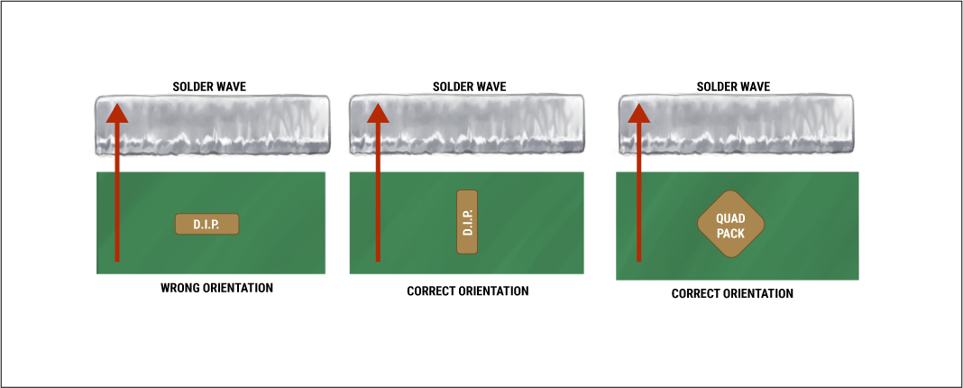
If the component is aligned parallel to the wave, an elastic membrane (we can also think of it as a solid web or stretchy sheet) forms between the leads and the wave. The membrane stretches like a taffy pull as the assembly moves farther from the wave.
Eventually, the membrane breaks. Most of the solder draws back to the wave because of surface tension (see item 3 above), but the rest snaps to the leads (surface tension again). Because the leads are close together, however, just a small amount of excess solder can join the leads and create a bridge (i.e., short).
If the I.C. is perpendicular to the wave, however, each lead comes out of the wave in sequence, and the solder flows down the row rather than clinging to each lead until the final lead. When the last lead emerges from the wave, the solder membrane is more like a thin elastic band rather than a sheet. When the band snaps, only a small quantity of solder clings to the lead, and bridging is prevented.
(The orientation rule changes for rectangular components such as quad packs that have leads on four sides. They should be rotated 45°.)
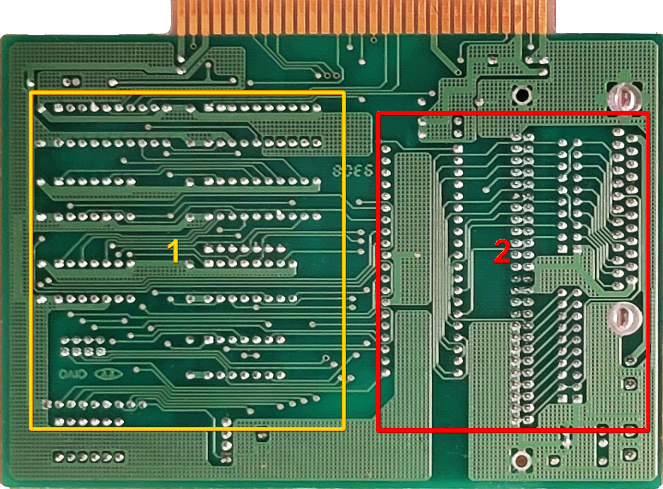
If bridging continues even with proper component alignment and machine operation, adding a non-functional pad at the trailing edge of the leads can draw extra solder and prevent bridging. The term for the non-functional pad is “solder thieve” because it takes away solder.
Alignment is critical, but don’t forget the last sentence of item 3: oxidation of the solder’s surface kills the surface tension that breaks bridges and prevents spikes.
Sierra Circuits employs advanced technologies and software to fabricate and assemble your board as per IPC-610-A and J-STD-001 guidelines.
Visit our PCB manufacturing capabilities to learn more.
Evolution of wave soldering machines
Wave soldering began with simple symmetrical waves (1950s) that soldered through-hole boards but caused bridging and inconsistent solder distribution. It evolved into flatter symmetrical waves and later asymmetrical waves (1970s), improving solder drainage, reducing defects, and enabling reliable through-hole soldering. With surface-mount technology, dual-wave systems (chip + laminar), nitrogen environments, and selective pallets were introduced to handle hybrid assemblies containing both SMD and through-hole components.
1. The first wave soldering machine
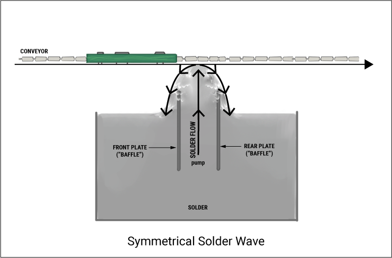
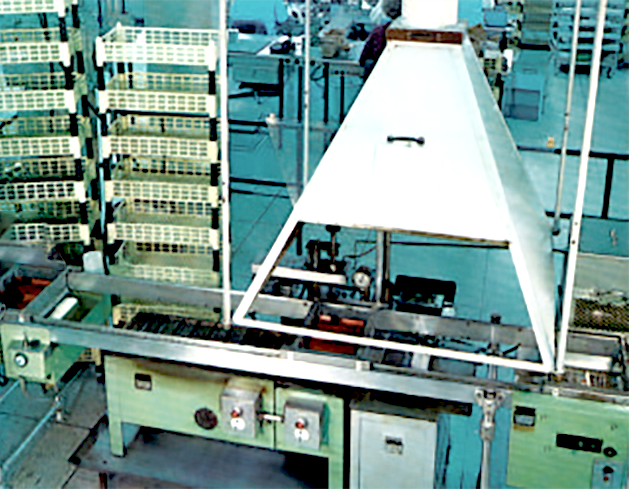
The first wave soldering equipment could not have been simpler. Plates (“ baffles”) were placed in a tank of melted solder (the “pot”). Solder pumped up between the baffles formed a narrow wave with the solder flowing quickly and equally over the front and back plates (i.e., a “symmetrical wave”), in essence, a dam except with flow to the back as well as the front.
The assembly was dipped in a pan of flux, then placed on a flat conveyor. As the conveyor moved the fluxed assembly over the wave, solder flowed across the bottom of the PCB. All going well, the result was solder connections between leads and pads across the entire board.
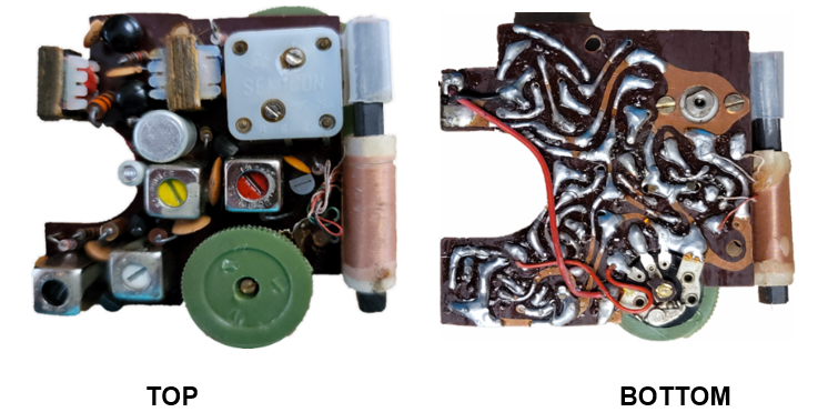
This wave-soldered transistor radio from 1958 shows typical results. The exposed copper areas result from inconsistent height across the width of the wave. The large pads, traces, and leads retained a lot of solder, and only the wide spacing between conductors prevented massive bridging.
Soldering irons were still needed to clear bridges and spikes and add solder where necessary, but the amount of labor was small compared to what had been needed before printed circuits.
The skinny symmetrical wave performed adequately for crude circuitry, but as component technology evolved rapidly and designers needed to pack more components into less space, the skinny symmetrical wave’s deficiencies became impossible to ignore.
In addition to stabilizing the wave profile, it was necessary to reduce the speed at which the assembly emerged from the wave so solder would have more opportunity to drain into the bath rather than clinging to the circuitry.
2. Second generation: Still symmetrical
Although it may seem that conveyor speed would determine the speed at which the assembly separates from the solder, that is not the case. With a symmetrical wave, the speed at which the solder falls away from the wave crest is so great that conveyor speed is almost irrelevant. Therefore, two machine modifications were introduced, neither of which involved reducing conveyor speed:
First, the distance between the baffles was increased to flatten the wave and slow the movement of solder on the wave crest. Second, the conveyor was tilted (6° was common) so the assembly would leave the wave at the relatively flat crest where solder flowed most slowly.
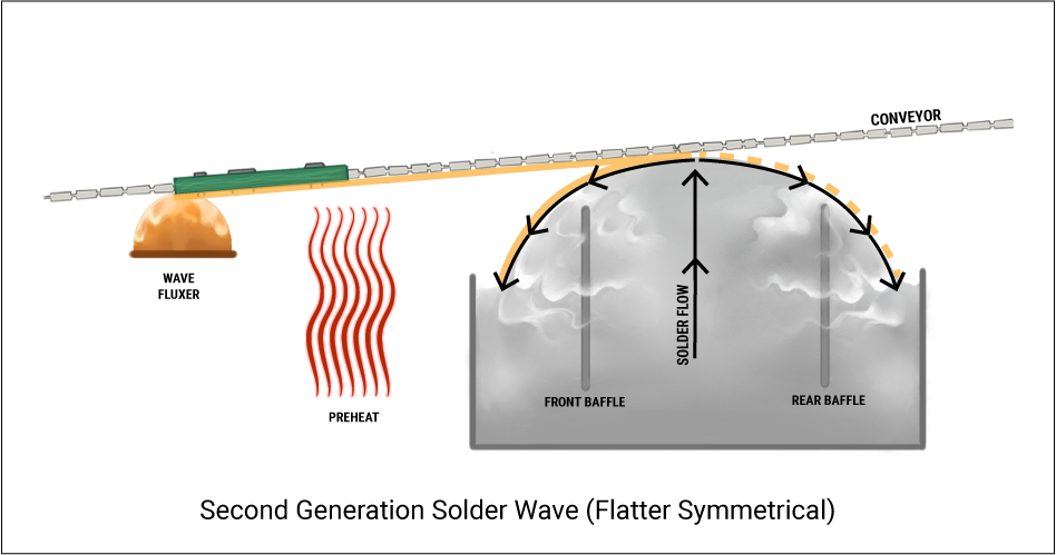
In-line fluxing replaced manual fluxing, although the flux was applied in a liquid wave that flooded the PCB. The excessive flux increased materials costs, of course, but cleaning heavy concentrations of rosin after soldering cost far more. The liquid wave would ultimately be replaced, first by foam fluxers, then by spray.
(Rosin’s function is often believed to be the removal of oxides from surfaces to be soldered. But that is not the case. Although rosin, which is derived from the sap of pine trees, does contain a little organic acid, that acid is too mild to remove any meaningful oxides. More robust acids are added to perform deoxidation.
Rosin coats the deoxidized surface, forming a barrier that prevents oxygen from reaching and reoxidizing the deoxidized metal. Where liquid is required for easier application, solvent is added to the rosin/acid combination. As we will discuss shortly, heavily concentrated rosin flux was useful only during the third generation of wave soldering.
For virtually all uses today, and certainly for hand soldering, more than slight amounts of rosin provide no benefit and result in expensive attempts to remove the residues after soldering. Many modern fluxes replace the rosin with other materials like glycols and glycerin that are less messy and can be removed with water.)
Heaters were introduced to drive off solvents, activate the flux, and gradually increase PCB temperature so the circuitry would not experience thermal shock (abrupt changes in dimensions of the circuit board when subjected to the high solder temperature).
When the assembly entered the solder wave, the pressure of the wave displaced much of the flux. Most flux that survived passage through the wave was flushed away during exit from the wave.
To ensure complete contact between the solder and circuitry without solder flowing over the top of the PCB, the wave height was set to come about halfway up the thickness of the circuit board.
The assembly emerged from the wave into atmospheric oxygen, so the surface of the solder oxidized, and surface tension was lost. (Remember the importance of surface tension, the desire of the solder to draw back into a ball, in the prevention of bridging.)
Mixing oil (peanut oil, originally) into the wave was briefly attempted on the theory that the constant flow of oil would produce a continuous coating between the solder and oxygen. The actual result was less successful. The amount of oil varied tremendously across the width of the wave, ranging from completely absent (failing to prevent bridges) to so great that it prevented solder from making contact (causing opens).
Making matters worse, the oil was dirty, smelled, and added to the materials cost. The experiment did not last long, although the approach was briefly revived later during experiments with wave soldering surface mount components.
Circuit assemblies grew increasingly complex with more components in less and less space. Ultimately, even the combination of a flatter wave and an angled conveyor could not prevent serious excess solder issues. Every wave solder machine was followed by teams of touch-up operators to fix the defects.
3. Third generation: The wave becomes asymmetrical
The next evolution (patented by Electrovert in 1975) was engineering genius. Making the front baffle shorter than the rear baffle and adding a curved forward-facing plate resulted in a flat wave where all solder flow occurs over the front baffle.
Although the top of the wave is slightly above the top of the rear baffle, surface tension keeps the solder from flowing over the back. When properly configured, the top of the wave is perfectly motionless until the assembly enters the wave.
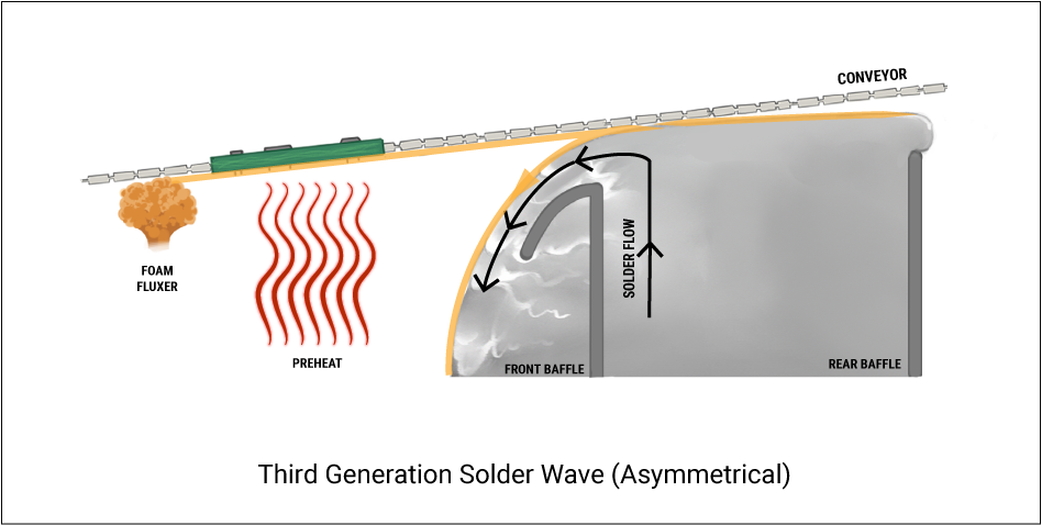
As the assembly enters the wave, the genius behind the wave design becomes evident. If the wave and conveyor heights have been set properly, about half the thickness of the PCB enters the solder wave, and solder begins to move across the top of the wave at the same speed as the PCB.
Solder displaced by the PCB begins to flow over the rear baffle. Since the assembly and surface solder are moving at the same horizontal speed, the only separation between the PCB and solder is vertical.
If the conveyor is moving at 6 ft/min, the speed at which the PCA separates from the solder is only 0.264 ft/min. The critical speed of separation is only a small fraction of the conveyor’s total speed, ample time for excess solder to drain off.
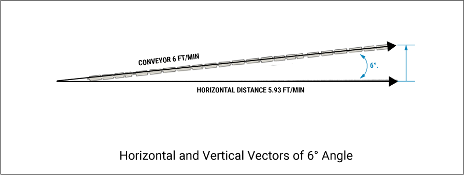
At the same time, something of great importance is happening with respect to the flux (which was now being applied as a foam rather than a solid wave). As with the symmetrical wave, most but not all of the flux solids are washed away by the forward-flowing solder at the front of the wave.
Instead of being washed away as happened with the symmetrical wave, however, the flux that survives stays on the flat solder surface and forms a barrier between the solder and oxygen (i.e., air). The flux barrier protects the solder from oxidizing. Being free of oxides, the solder maintains its high surface tension as the PCB separates from the wave and breaks the web that might otherwise cause bridging.
This is the time when heavy concentrations of rosin in flux proved useful. More rosin going into the wave improved the chances of rosin after the wave. Liquid fluxes containing high concentrations of rosin continue to be sold, but they are remnants of this era in wave soldering.
Except for wave soldering assemblies that have no SMDs on the wave side of the PCB, so much rosin provides no benefits, but the messier assemblies require expensive post-soldering cleaning.
The flat, asymmetrical wave achieved both objectives of slow separation from the solder and a barrier to oxygen. Provided all multileaded devices were correctly oriented to enter the wave head-on rather than sideways (not always possible, especially with edge connectors), wave soldering nirvana had been reached. Perfect soldering was easy, and life was great.
Then surface mount devices (SMDs) arrived, and life got complicated.
4. Fourth generation: SMDs and chip waves
At first, surface-mount parts were restricted to the top of the PCB. The surface-mount parts were placed and soldered before the insertion and wave soldering of through-hole components. That was easy. Inevitably, though, designers began placing surface-mount parts on both sides of the PCB. The combination of SMDs and through-hole components became known as “hybrid assembles.” And PCAs created significant new problems.
You can read about the 8 common errors in SMT.
First, the SMDs needed to be fastened to the circuit board as it passed through the wave. So, glue was applied to the PCB at the points where the component body would be located. Then the components were placed. The equipment to apply glue was costly and required constant maintenance.
The glue cost money and needed curing, which meant adding even more equipment (typically heaters or UV, depending on the type of glue) and increased processing time. And, perhaps worst of all, achieving the proper balance between too little glue (parts would disappear into the solder) and too much (contamination of pads and other surfaces to be soldered) proved to be quite difficult, and that difficulty only increased as the parts kept shrinking.
Adding to the complexity, fluid dynamics differ between through-hole and SMD assemblies. With a pure through-hole assembly, there are no obstacles to prevent the solder from making complete contact with all the component leads.
The through-hole lead plows into the solder wave like the prow of a boat. Then, interatomic attraction draws the solder around the deoxidized lead and up a plated barrel. SMDs, on the other hand, have bodies that cause solder to flow over the trailing edge like a waterfall that may not contact leads at the back of the component, as with through-hole packages, alignment matters.
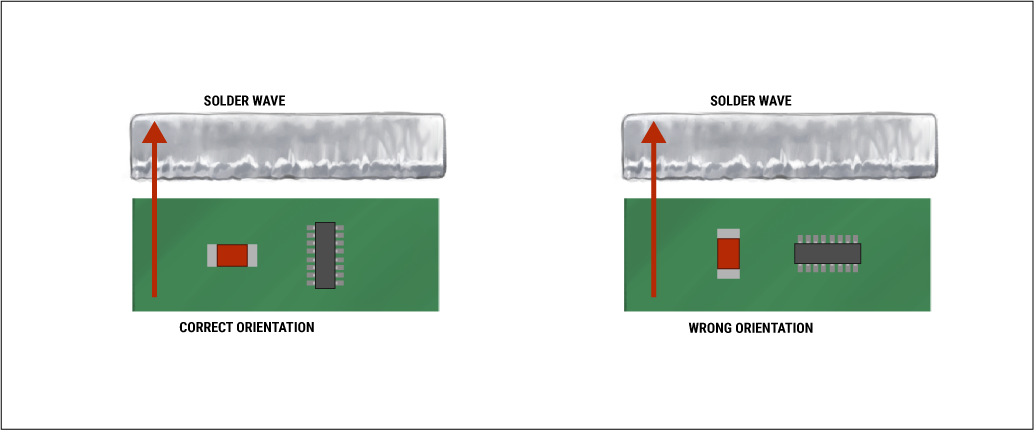
Technology places limits on what even the best layout engineer can achieve, however. Although properly aligned, some small parts inevitably had to be placed behind larger parts, resulting in block solder from reaching the smaller components.
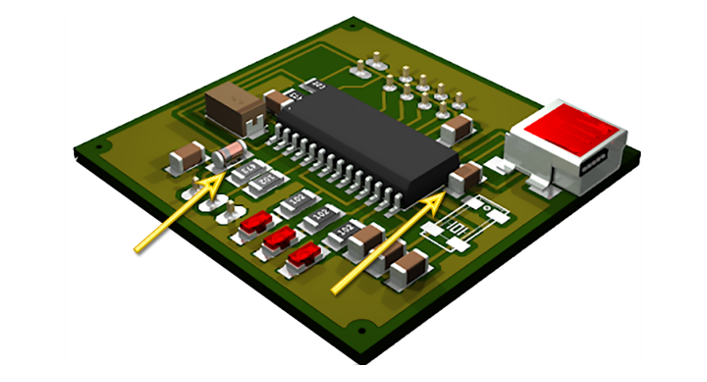
Solder skips also occurred because of trapped air or flux. The high rosin concentration fluxes that had been so helpful in preventing excess solder became liabilities with the introduction of SMDs.
Unsoldered connections (opens) were common and, even worse, difficult to detect both visually and by test. (Even without solder, sufficient mechanical contact might exist between the component and pad to fool electrical tests.)
Solder skips became the dominant issue in wave soldering and resulted in the introduction of a new, turbulent (“chip”) wave before the original asymmetrical wave. The turbulence forced the solder to move aggressively in three dimensions, pushing aside flux and overcoming the shadowing effects of component bodies.
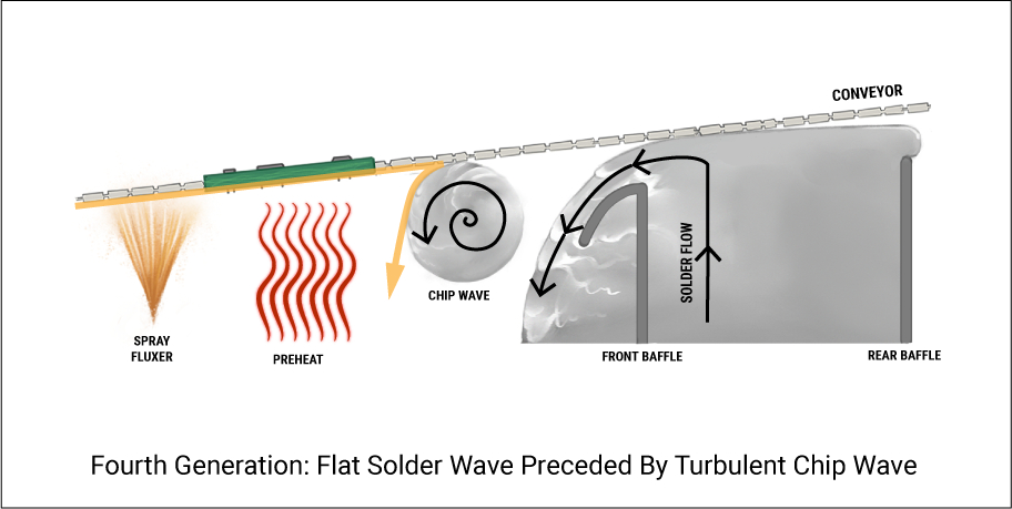
Emerging from the chip wave, all the intended connections are indeed soldered. However, a new problem arises. The turbulence causes rapid separation of the assembly from the wave and sweeps away the flux. (Around this time, the foam fluxer gave way to spray nozzles that could better control the volume and coverage of flux.) The assembly leaves the first wave covered with bridges.
The function of the asymmetrical wave (now more commonly called the “second wave”) changed from making solder connections to removing the bridges produced by the first wave. (The second wave also provided additional heat to help complete the solder fill of plated holes.) But the chip wave meant there could be no flux solids when assemblies left the second wave. So, bridging once again became a serious problem.
There are not many ways to help flux survive reaching the exit point of the second wave, but substituting matte solder mask for semi–gloss or gloss solder mask often makes a small but meaningful difference. The improvement won’t be dramatic, but even a little help is always better than none.
The wave solder machine manufacturers tried a couple of ideas to solve the resurrected excess solder problems, generally without success. The idea of mixing oil from the symmetrical wave era was tried again, but disappeared rather quickly because of the same issues (dirty, smelly, costly, and prone to blocking solder connections) that oil had caused years earlier.
Hot air knives (heated air blown at high pressure at the point of separation between PCA and solder) were tried as well. Again, the results were not good. Blowing away excess solder tended to remove needed solder, as well. Not infrequently, the entire component would disappear.
Finally, the industry decided to replace normal oxygen-containing air with an inert gas, nitrogen. Nitrogen is not truly inert but reacts with very few other elements, none of which are found in the typical electronics plant.
So, for the purposes of electronics assembly, nitrogen is “insert.” And nitrogen is plentiful; it makes up roughly 78% of the air around us (oxygen accounts for about 21%). The logic is inescapable, but actually achieving sufficiently low oxygen levels to make a meaningful difference (around 500 parts per million, which is only 0.05%) presents several engineering challenges.
Oxygen is denser than nitrogen. Consequently, nitrogen must be injected constantly at high volume, or oxygen will simply resume its place. (A sealed chamber would not require nitrogen replacement but would not allow for the conveyance of the assemblies, either.) The best option is generally a very long tunnel with nitrogen infusion in the center and air flow out the ends.
Although nitrogen use has become very common, its purpose often remains poorly understood. The general belief is that nitrogen’s role is dross reduction. However, while dross formation is reduced, that alone is not normally sufficient to cover the cost of gas and sophisticated equipment. Far more importantly, nitrogen compensates for the missing flux.
If sufficient oxygen can be displaced, prevention of excess solder in a dual wave system can perform as well as the single asymmetrical wave system in the pure through-hole era.
One quirk of nitrogen does deserve comment. If the oxygen level drops to around 0.02% or less, solder tends to drop to the wave rather than gradually peeling back. The solder can act like a stone dropped in water and splash back up to the circuitry. In other words, oxygen in general causes soldering problems, but an almost complete absence creates entirely new issues.
5. Fifth generation: Selective pallets
Gluing SMDs fell out of fashion within a very few years. The usual practice today is solder paste reflow (generally through ovens) for both sides of the PCB. The assembly is placed in a fixture (“pallet”) that covers the SMDs on the solder wave side. Openings in the pallet allow insertion of the through-hole parts for wave soldering.
During passage through the wave, the exposed leads are soldered while the SMDs previously soldered to the bottom of the PCB are protected.
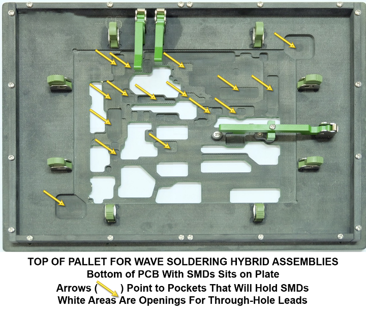
Pallets make wave soldering of hybrid assemblies possible, but there are serious liabilities. The most obvious is extra handling because the assemblies must be placed in pallets at the start of the conveyor and removed at the end. (Handling a hot pallet is no one’s idea of fun.) Extra handling also increases throughput time (reduces output).
Moreover, the pallets themselves are expensive and tend to wear out quickly because of contact with the solder and constant temperature cycling. Different types of PCAs require their own pallets. Flux residues must be removed. Latches break.
And then there are soldering issues, of which there are many, including no solder (skips), excess solder (bridges, webbing, solder balls), and insufficient vertical fill of plated through-holes. Skips result primarily from solder surface tension that prevents consistent contact with leads located next to the walls surrounding the openings for through-hole leads.
Increasing chip pressure can force the solder into tight spaces and up to the edges of through-hole openings, but it adds the risk of solder flowing into the SMD pockets. The rapid solder flow with the chip wave also means rapid separation of parts from the solder that causes bridges.
Given the greater ability of in-circuit test to catch bridges than shorts, the chances of these defects reaching a customer are not great, but clearing bridges is an expensive manual operation.
Wave soldering hybrid assemblies will always result in defects. However, a few ways to reduce defects do exist, including:
- Make the openings as large as possible. (In other words, minimize the area covering SMDs.) Design plays an important role in enabling this, but, as always, technology and circuitry requirements constrain even the best designers.
- Make the pallet plate as thin as possible. However, the thickness is dictated by the highest profile surface mount components. (The pallet plate must be thick enough that enough to cover the component after routing out the pocket that will contain the part.)
- Chamfer the edges of the through-hole openings.
- Cut channels in the pallet perpendicular to the solder wave, reducing resistance to solder flow.
- Keep individual through-hole leads as far as possible from the walls of the openings.
- Make pads near the pallet openings larger to increase the probability of contact with solder.
Nothing beats a single asymmetrical solder wave (generally with top-side preheaters as well as the standard heaters beneath the conveyor) for pure through-hole assemblies. With proper design, flux, and conveyor speed, defect-free soldering is achievable without nitrogen or much effort.
Unfortunately, the days of pure through-hole assembly are pretty much behind us. Like it or not, through-hole components generally are accompanied by surface mount components on both sides of the PCB.
Wave soldering hybrid assemblies almost always requires use of selective soldering pallets. For simple assemblies with lots of clearance between through-hole and surface mount parts (ideally with components grouped by type rather than spread randomly across the PCB), pallets can work rather well, albeit with more handling and cleaning required.
But, increasingly, wave soldering hybrid assemblies (with pallets or not) makes less sense than soldering through-hole parts by hand or mini-wave selective solder. I will discuss these other approaches in future columns.
Blog written by:
James A. (Jim) Smith, PhD ABD, President, Electronics Manufacturing Sciences, Inc.
jsmith@emsciences.com
Have queries regarding wave soldering? Post them on our community, SierraConnect. Our design experts will answer them.




Start the discussion at sierraconnect.protoexpress.com