


Contents
Routing differential pairs is a crucial step in designing high-speed PCBs, as it directly impacts the signal integrity. KiCad offers features like differential pair routing, length tuning, and skew matching to ensure both traces have identical length, width, and proper spacing, minimizing signal interference.
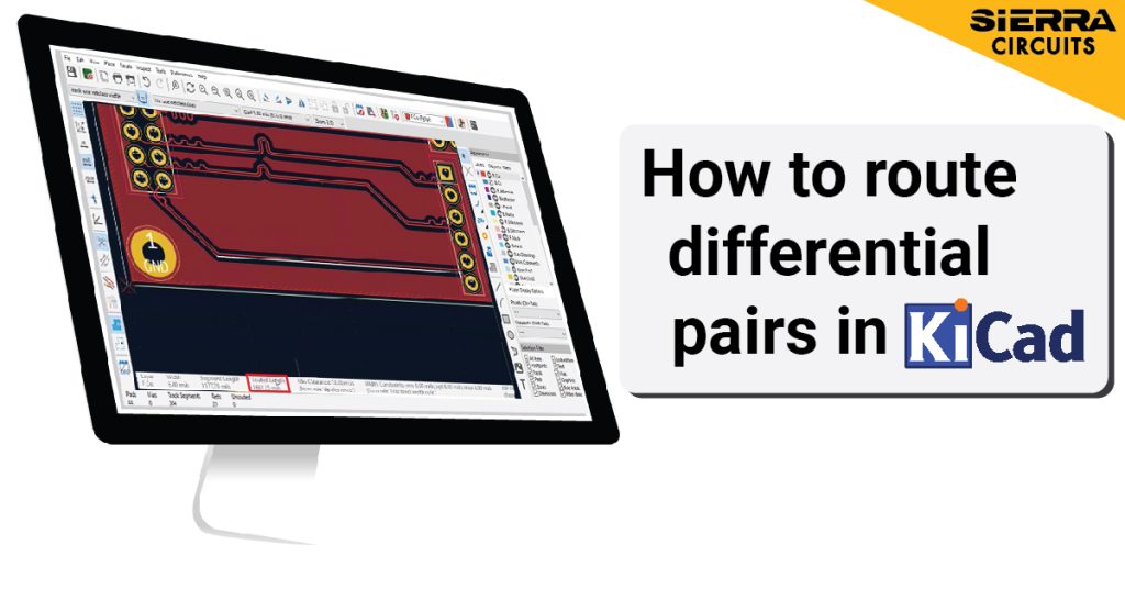
In this KiCad tutorial, you will learn the steps to route differential pairs in KiCad, ensuring accurate signal timing, length matching, and skew control.
Routing a differential pair in KiCad
Step 1: Choose the layer to route the differential pair
Before routing a differential pair, confirm that you’re on the correct layer. To route on the bottom layer, select Bottom.Cu in the layer selector.

Step 2: Select the differential pair tool
Navigate to Route –> Route Differential Pair from the menu.

Step 3: Route the traces
Select the starting point of the pair, typically from a pad or via, and click to start routing. Guide the traces along the desired path. KiCad will automatically maintain the specified gap between the two traces.

To learn the process of autorouting your PCB, read how to autoroute a PCB layout in KiCad using FreeRouting plugin
Step 4: Check the skew
Ensure the skew between the two lines of the differential pair does not exceed your set tolerance (typically around 5 mil). This can be adjusted in the rule settings, which we have discussed in the matching skew between traces section.
For the final connection, you can use a single trace to make it easier to complete the routing.
For step-by-step guidelines on designing a PCB using KiCad, download our eBook.

KiCad Design Guide
10 Chapters - 161 Pages - 180 Minute ReadWhat's Inside:
- Creating a component symbol library
- Setting up board parameters and rules
- How to route differential pairs
- How to place of components
Download Now
Length tuning the differential pair
You must length-match the differential pairs to ensure signal integrity in high-speed PCB designs. Follow these steps to length-match differential pairs using KiCad.
Step 1: Set up length-matching rules
Before tuning, you need to define the length-matching parameters in Board Setup.
To access the Board Setup dialog, click the Board Setup icon in the top toolbar or navigate through File –> Board Setup.

In the Board Setup, click on the Length-Tuning Patterns section. Set the parameters for single-track, differential pairs, and differential pair skews.
Define the amplitude, the spacing for serpentine patterns (ideally 3W), and the corner style (e.g., Fillet).

The spacing is calculated from edge-to-edge of the traces rather than center-to-center to achieve the desired 3W spacing accurately.
For more expert tips on high-speed design, read how to create a schematic for high-speed designs in KiCad.
Step 2: Create and assign a differential pair class
Create a new net class for your differential pairs and set the trace width and clearance according to your design requirements. Next, configure the differential pair width and gap (clearance between the traces).
Go to the Net classes section in the Board Setup and assign a class to the differential pairs.

Ensure your minimum track width in the constraint manager is less than or equal to the differential pair width. If this is not set correctly, KiCad may not apply the rules as expected, leading to routing errors.


Step 3: Calculate and set length matching tolerances
After routing the traces, check the routed length for each trace. Identify the longest trace in your differential pair.

Use its length as a reference to set custom rules under Design Rules in the Board Setup.

For example, if the longest trace is 1661.25 mil, set the maximum length to 1662 mil and allow a tolerance of ±10 mil. This means the minimum length should be set to 1652 mil.
All traces within this class will be evaluated against these minimum and maximum length limits, and any trace falling outside this range will trigger an error.
To receive an instant cost estimate for your PCB design without exiting KiCad, install the KiCad Quote Plugin.
Step 4: Perform length tuning
Once the rules are set, use the length tuning tool to adjust the shorter trace. Go to Route —> Tune Length of a Differential Pair from the menu.


The tool will display the current length, and as you drag to adjust, it will update the length to meet the minimum and maximum requirements you’ve set.

When the length falls within the specified range, click to finalize the tuning.
After tuning, verify that all differential pairs meet the length-matching criteria. If the traces don’t match the required length, KiCad will flag them, allowing you to make further adjustments.
Download our KiCad 9 Step-by-Step Guide to quickly understand the PCB design workflow.

KiCad 9 Step-by-Step Guide
6 Chapters - 41 Pages - 30 Minute ReadWhat's Inside:
- A complete KiCad 9 workflow from project creation to production file generation
- Step-by-step guidance on creating custom libraries and linking symbols to footprints
- Practical design checks: ERC and DRC
- Best practices for generating a clean BOM and fabrication-ready Gerber files
Download Now
Matching skew between traces
Skew matching is an essential step when working with differential pairs. It ensures that the signals on the pair’s positive (P) and negative (N) traces remain synchronized. KiCad provides tools and custom rules to help achieve precise skew matching.
Step 1: Access the board setup
Navigate to File —> Board Setup or click the Board Setup icon in the top toolbar.

Step 2: Define skew matching rules
In the Board Setup dialog, go to Design Rules —> Custom Rules. Set the skew constraint rule. This rule is specifically for skew matching within differential pairs.
For example, set the minimum skew as -5 mil and the maximum skew as +5 mil. This configuration means that the length difference between the P and N traces should not exceed 5 mil in either direction.

If the longest trace in the pair is 100 mil, the shorter trace must be between 95 mil and 100 mil. The rule checks each trace in the pair individually, ensuring that neither exceeds the defined skew limits.
Make sure the skew rule is only applied to coupled differential pairs. In the Custom Rules section, specify that the rule applies to traces that belong to the same differential pair.
KiCad version 9 introduces skew management features for differential pairs. This allows you to set advanced rules to minimize skew and enhance signal integrity in high-speed designs. Discover more enhanced features in KiCad version 9: exploring the new features.
Need help in designing reliable PCBs? Our engineering team can help you with impedance-controlled routing, length matching, and signal integrity
You can book a meeting with our experts or call us at +1 (800) 763-7503.

Step 3: Tune the skew of the differential pair
After setting up the skew constraint, you can proceed with tuning the skew. Click on Route –> Tune Skew of Differential Pair. This allows you to adjust the trace lengths within your skew tolerance.

Click on the differential pair to verify the current skew.

If the skew exceeds the set limit, adjust the trace by pulling it to reduce the length difference and match it more closely with the other trace.
If there are multiple differential pairs, space them at least 5W apart, where W represents the width of the differential pair.
To learn the steps for routing standard traces in KiCad, see how to route a PCB in KiCad.
Have queries on PCB design, assembly, and manufacturing? Post them on our forum, SierraConnect; our experts will answer them for you.

About Pooja Mitra : Pooja Mitra is an electronics and communication engineer. With an experience of over three years in the PCB industry, she creates industry-focused articles that help electrical and PCB layout engineers.


Start the discussion at sierraconnect.protoexpress.com