


Contents

On-demand webinar
How Good is My Shield? An Introduction to Transfer Impedance and Shielding Effectiveness
by Karen Burnham
A PCB transmission line is a type of interconnection used for moving signals from the transmitters to the receivers on a circuit board. It is composed of two conductors: a signal trace and a return path, which is usually a ground plane. The two conductors are separated by a dielectric material.
The alternating current that runs on a transmission line usually has a high frequency to manifest its wave propagation nature. The key aspect of wave propagation is that the transmission line has an impedance at every point along its length. Furthermore, if the line geometry is the same along the length, the line impedance is uniform.
We call this line a controlled impedance trace. Non-uniform impedance causes signal reflections and distortion. Therefore, at high frequencies, transmission lines need to have a controlled impedance to predict the behavior of the signals.
It is crucial to pay attention to the transmission line effects in order to avoid signal reflections, crosstalk, and electromagnetic noise.
Highlights:
- Controlled impedance is critical for preventing signal reflections, crosstalk, and electromagnetic interference in high-speed PCB designs.
- Microstrips are routed on outer PCB layers, while striplines are embedded between reference planes.
- Coplanar waveguides place the signal trace and ground conductors on the same PCB layer.
- Transmission line effects become significant when the signal propagation delay is comparable to the signal’s rise/fall time or operating frequency.
What are the types of PCB transmission lines?
There are three types of transmission lines used in PCBs: microstrips, striplines, and coplanar waveguides.
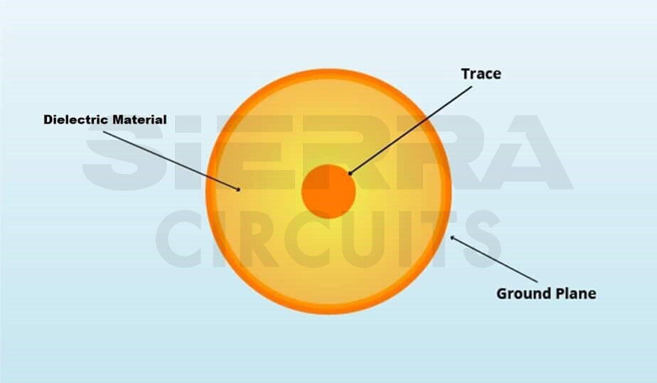
Microstrip transmission line: It is composed of a single uniform trace located on the outer layer of a board and parallel to a conducting ground plane. This plane provides the return path for the signal. The trace and the ground plane are separated by a certain height of PCB dielectric, as shown in the image below.

Stripline transmission line: It is composed of a uniform trace located on the inner layer of a circuit board. The trace is separated on each side by a parallel dielectric layer and then a conducting plane. So, it has two current return paths – reference plane 1 and reference plane 2.

Coplanar waveguide: A coplanar waveguide structure has a signal trace and return path on the same layer of the board. The signal trace is at the center, surrounded by two adjacent outer ground planes.
This structure is called “coplanar” because these three flat structures are on the same plane. The dielectric is located underneath. Both microstrips and striplines may have a coplanar structure. Below is a coplanar microstrip waveguide with a ground plane:

To learn more about controlled impedance, see why controlled impedance really matters
Example of a coaxial cable (which is not a PCB transmission line)
A coaxial line has a circular shape and is not a circuit board transmission line. This circular cable is composed of a central wire conductor and an outer conductor for the return path. The space between the two conductors is filled with a dielectric material. The outer conductor wire completely surrounds the signal wire.
Coaxial lines are mostly used as cables for high-frequency applications, such as television, etc. These cables must have a uniform conductor geometry and dielectric properties throughout their length.
It is essential to keep in mind that a PCB transmission line is composed not only of the signal trace but also of the return path. Usually, it is an adjoining ground plane or a coplanar conductor, or a combination of both.
When is an interconnection considered a transmission line?
An interconnection must be treated as a transmission line when its signal propagation delay is significant compared to the signal’s rise/fall time or the period of its highest-frequency component.
This scenario typically occurs when the propagation delay is comparable to one-fourth of the wavelength of the signal’s highest-frequency component. In such cases, transmission line effects such as reflections and impedance mismatches must be considered to preserve signal integrity.
Two very important properties of a transmission line are its characteristic impedance and its propagation delay per unit length. Signal reflections, crosstalk, and electromagnetic noise will occur if the impedance is not controlled along its entire length. It can also occur when the line is not terminated by the right value of impedance. This affects the signal integrity of the circuit board.
Consider the signal frequencies (analog) or the data transfer rates (digital) are less than 50 MHz or 20 Mbps. Here, the time taken by a signal to travel from its source to its destination would be very small (< 10%). This is in comparison to the time period of one-fourth of a wavelength or the fastest rise time of a digital pulse signal.
In this case, you can estimate the interconnect by assuming the signal at the destination follows the signal at its source at the same time. In such a low-speed scenario, the PCB signal can be analyzed by conventional network analysis techniques. We can also ignore any signal propagation time or transmission line reflections, etc.
However, when dealing with signals at higher frequencies or higher data transfer rates, the signal propagation time between the source and the destination cannot be ignored. Therefore, it is not possible to analyze the behavior of such high-speed signals using ordinary network analysis techniques. The interconnects need to be considered as transmission lines and analyzed accordingly.

PCB Transmission Line eBook
5 Chapters - 20 Pages - 25 Minute Read
What's Inside:
Download Now
How to predict the signal behavior on microstrips and striplines?
At high frequencies, calculating signal propagation speed and propagation delay, along with maintaining controlled impedance, helps accurately estimate signal performance on microstrips and striplines.
At high frequencies, transmission lines need to have a controlled impedance to predict the behavior of the signals and avoid integrity issues.
This is the reason why you need to know at which speed signals propagate on transmission lines and the time they take to do so. We will give you a few equations to calculate the signal speed and the propagation delay for both stripline and microstrip structures.
What is signal speed?
Signal speed is the velocity at which an electromagnetic signal propagates along a transmission line.
Let’s first discuss the speeds at which signals propagate on a PCB interconnect.
Electromagnetic signals travel in a vacuum or air at the same speed as light, which is:

A signal travels on a transmission line at a slower speed, affected by the material’s dielectric constant (Er). The relations for calculating the signal speed on a PCB are given below:
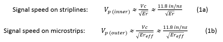
Where:
Vc is the velocity of light in vacuum or air
Er is the dielectric constant
Ereff is the effective dielectric constant for microstrips. Its value lies between 1 and Er. It is approximately given by:
Thus, signal speed is less than that of air. If Er ≈ 4 (like for FR4 material types), then the signal speed on a stripline is half that in air, i.e., it is about 6 in/ns.
Henceforth, we can use Vp to denote the speed of signals on a PCB.

High-Speed PCB Design Guide
8 Chapters - 115 Pages - 150 Minute ReadWhat's Inside:
- Explanations of signal integrity issues
- Understanding transmission lines and controlled impedance
- Selection process of high-speed PCB materials
- High-speed layout guidelines
Download Now
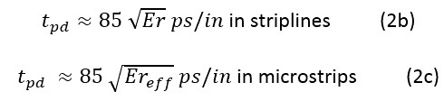
What is propagation delay?
The propagation delay is the time taken by a signal to propagate over a unit length of the transmission line:
Where V is the signal speed in the transmission line. In vacuum or air, it equals 85 picoseconds/inch (ps/in).
On transmission lines, the propagation delay is given by:

What materials are used in transmission lines?
The most used substrates are Isola 370HR, Isola I-Speed, Isola I-Meta, Isola Astra MT77, Tachyon 100G, Rogers 3003, and the Rogers 4000 series.
The signal speeds and propagation delays for a few board materials are given in the table below:
| Material | Er | Ereff | V (in/ns) microstrip | V (in/ns) stripline | tpd (ps/in) microstrip | tpd (ps/in) stripline |
|---|---|---|---|---|---|---|
| Vacuum or air | 1 | 1 | 11.8 | 11.8 | 85 | NA |
| Isola 370HR | 4.0 | 2.92 | 6.90 | 5.9 | 145 | 170 |
| Isola I-SPEED | 3.64 | 2.69 | 7.20 | 6.18 | 139 | 162 |
| Isola I-META | 3.45 | 2.57 | 7.36 | 6.35 | 136 | 158 |
| Isola Astra MT77/ Tachyon 100G/ Rogers 3003 | 3.0 | 2.28 | 7.8 | 6.8 | 128 | 147 |
| Rogers 4000 series | 3.55–3.66 | 2.63–2.70 | ~7.20 | ~6.20 | ~139 | ~161 |
What are the important features of a circuit board transmission line?
Critical length, controlled impedance, and signal rise/fall time are the key parameters used to evaluate transmission line behavior in high-speed PCB designs.
As mentioned above, for high-speed or high-frequency signals, we need to consider the transmission line effects. We can use a few thumb rules:
In the case of high-frequency analog signals, let the maximum frequency content of the signal be ![]()
What is the critical length of a signal line?
For analog signals, the critical length, lc, is defined as one-fourth of the wavelength of the highest signal frequency contained in the signal.
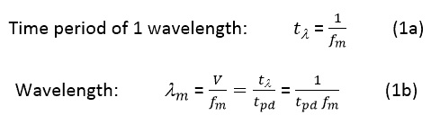
In the case of digital signals, the fastest rise/fall time of a signal pulse is the most important parameter. It defines the transition time from one logic level to another logic level. Basically, the transition time of the data bit. For digital signals, the critical length, lc, is defined as the line length over which the signal propagation time is half of the fastest rise/fall time of the signal pulses.
If tr = fastest rise/fall time of the digital signal, the time of signal propagation over the length lc is tpd (propagation delay).
This definition implies that the signal should be able to travel from the source over a length lc of the line. This signal should return over the same length back to the source point in a total time equal to the rise/fall time, tr.
Equations 2a and 2b are related if we consider the highest frequency content in a digital signal’s rise/fall time.
The highest frequency content in a digital signal of rise/fall time tr is given by (as per Fourier Analysis):
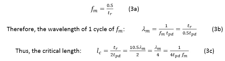
Which is the same as equation 2a.
What is a shortline?
If the line length is ![]() then, it is a short line. It is not necessary to consider its transmission line effects, nor to design it as a controlled impedance line.
then, it is a short line. It is not necessary to consider its transmission line effects, nor to design it as a controlled impedance line.
But if the line length is ![]() then, it is necessary to consider the transmission line effects and to design such lines as controlled impedance lines.
then, it is necessary to consider the transmission line effects and to design such lines as controlled impedance lines.
Example:
If the fastest signal rise/fall time is: tr = 1ns, then, assuming the FR4 material with a dielectric constant Er = 4, ![]() and the critical length
and the critical length ![]()
Therefore, signal traces longer than 3/1.5 = 2 inches need to be designed as controlled impedance lines. Note that tr of 1ns corresponds to a maximal signal frequency: ![]()
Need assistance in designing your circuit boards? Check out our PCB design support. Our engineers can help you with material selection, stack-up, component placement, and routing.

How to estimate the rise/fall time from data transfer rate (DTR) or clock frequency?
DTR is usually ≥ 2 Fclock. Henceforth, it will be safe to use the following rule:
![]()
If we don’t know the signal rise/fall time, we can use the following rule:
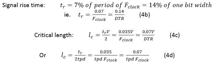
The data transfer rate is measured in bits per second (bps or bits/sec or b/s) and the clock frequency (Fclock) in Hz.
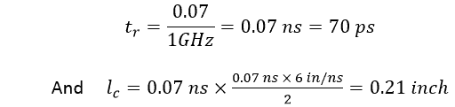
Example:
For Fclock = 1GHz or DTR = Gbps, and for a PCB material with Er = 4, we get:
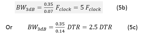
How to calculate the 3 dB bandwidth?
For a signal with rise/fall time tr, the 3 dB bandwidth is given by the following rule:
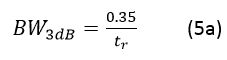
Therefore, for a clock of frequency Fclock, we get:
For proven design techniques to maintain uniform impedance, see designing transmission lines with controlled impedance in high PCB layouts.
How to analyze a PCB transmission line?
A printed board transmission line is analyzed using Maxwell’s electromagnetic equations and electromagnetic wave propagation theory. These methods accurately model the electric and magnetic fields generated by high-speed signals as they travel along the transmission line.
In these methods, we have to deal with electric and magnetic fields instead of the usual voltages and currents. The voltage between the signal line and its return path will generate an electric field and a current in the conductors. This, in turn, will create a magnetic field around them. Thus, voltage, current, electric, and magnetic fields all travel as waves along the transmission line.
There exists a close analogy between electromagnetic wave propagation, the propagation of voltages, and currents along a transmission line. As it is easier to think in terms of familiar voltages and currents rather than electric and magnetic fields, we should use the voltage/current analysis of the transmission line in the following treatment.
How is a PCB transmission line modeled for analysis?
A PCB transmission line is modeled as a series of infinitesimal-length segments, each represented by distributed resistance (R), inductance (L), capacitance (C), and conductance (G) per unit length. This distributed RLGC model enables accurate analysis of voltage, current, and signal propagation along the transmission line.
Each segment can be analyzed by network theory concepts at a particular point in space and time. Here, you can ignore the travel time in the infinitesimal segment as its length is extremely small.
In this analysis technique, we will be dealing with quantities like voltages and currents, and transmission line parameters like resistance, inductance, capacitance, and conductance. We will model an infinitesimal segment of a transmission line in terms of the following parameters:
R = the resistance per unit length (or p.u.l.) (R in Ohms p.u.l.)
L = the inductance p.u.l. (L in Henry’s p.u.l.)
C = the capacitance p.u.l. (C in Farads p.u.l.)
G = the conductance p.u.l. (G in Mhos p.u.l.)
We can denote the length of the infinitesimal transmission line by Δx.
Then, we can picture this transmission line segment as follows:
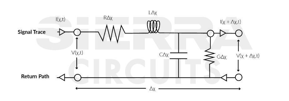
Where:
V(x,t) = signal voltage at location x at time t
I(x,t) = signal current at location x at time t
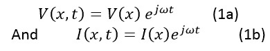
Let’s do the analysis of this circuit in the frequency domain. Here, we assume that the signals vary with time sinusoidally with an angular frequency ω, so that the time-varying part of V(x,t) and I(x,t) can be shown by the factor ![]() , and we now have:
, and we now have:
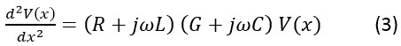
Using Kirchhoff’s laws on the above segment, we obtain the following relations:

And from these, by differentiation, we get:
A solution to this equation is:
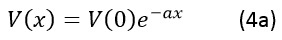
And from Equation 2,
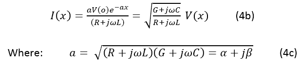
α has units of p.u.l.
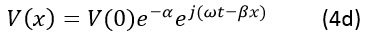
Multiply equation 4a by ![]() to reincorporate the time variations of the sinusoidal voltages and currents. Now the equations represent voltage and current signal waves traveling in the positive x-direction over the transmission line:
to reincorporate the time variations of the sinusoidal voltages and currents. Now the equations represent voltage and current signal waves traveling in the positive x-direction over the transmission line:
About the author: Atar Mittal is the Director and General Manager of the design and assembly division at Sierra Circuits. He is responsible for the design and development of strategies and process automation tools for complex printed circuit boards and assemblies. Atar is also currently engaged in the development of productivity tools for electronics designers that would have a tremendous impact on shortening the development time.
Need more information on circuit board transmission lines? Post your queries on our forum, SierraConnect. Our engineers will answer them.

About Atar Mittal : Atar Mittal is the General Manager and Director of the Design and Assembly Sierra Circuits division. He has a degree in Electrical Engineering from IIT Kharagpur and has worked in the electronics industry for over three decades.


Start the discussion at sierraconnect.protoexpress.com