Electroless palladium immersion gold (EPIG) is a nickel-free PCB surface finish suitable for high-speed and HDI designs.
Standard finishes like ENEPIG may not be the best choice for advanced boards with tight spacing. The electroless nickel (EN) layer in ENEPIG takes up space, leaving minimal clearance between conductors and increasing the risk of short circuits.
By eliminating the nickel layer, EPIG significantly reduces material build-up on traces, allowing for finer features and reduced clearances.
What is EPIG PCB surface finish?
It’s a lead-free, RoHS-compliant, and noble-metal-based coating designed to protect copper from oxidation and provide a reliable surface for soldering and wire bonding in printed boards.
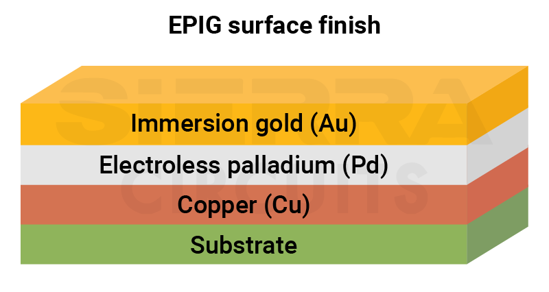
Table 1: Composition of EPIG
| Layer | Description | Material | Typical thickness |
|---|---|---|---|
| Electroless palladium (P-Pd) |
|
Phosphorous-based palladium | 0.10–0.15 µm |
| Immersion gold (RAI-Au) |
|
Reduction-assisted immersion (RAI) gold | 0.10–0.20 µm |
EPIG is one of the newer PCB surface finish technologies, introduced as an alternative to electroless nickel immersion gold (ENIG). Unlike ENIG, it eliminates the use of nickel, which can cause signal integrity issues in high-frequency circuits and trigger allergic reactions in users of certain medical devices.
While no formal IPC specification currently exists for EPIG, plating thickness should follow supplier-specific recommendations tailored to soldering and wire bonding needs.
If your board requires EPIG coating, clearly mention the same in your PCB fabrication notes.
EPIG vs. ENEPIG
| Feature | EPIG | ENEPIG |
|---|---|---|
| Nickel layer | Nickel-free | Contains a 5–6 µm-thick electroless nickel layer |
| Typical thickness | <0.35 µm | >5 µm |
| Solder joint formation | Directly on copper (Cu-Sn IMC) | On nickel (Ni-Sn IMC) |
| Clearance between conductors | Better due to less material buildup, allowing tighter spacing | The nickel layer reduces spacing and may cause shorts in dense layouts |
| Signal integrity | Superior (avoids skin effect and minimizes distortion) | Lower (nickel can degrade high-frequency signals) |
| Lead time | Faster | Slower due to the nickel plating process |
| Mechanical flexibility | High (ideal for flex circuits) | Moderate (nickel can crack during flexing) |
| Use cases | Suitable for high-frequency and magnetically sensitive designs | Widely used for general purposes, but less suitable for very high frequencies |
Download our eBook to learn how to select the right materials for your circuit boards.
PCB Material Design Guide
9 Chapters - 30 Pages - 40 Minute ReadWhat's Inside:
- Basic properties of the dielectric material to be considered
- Signal loss in PCB substrates
- Copper foil selection
- Key considerations for choosing PCB materials
Download Now
Electroless palladium immersion gold surface finish process
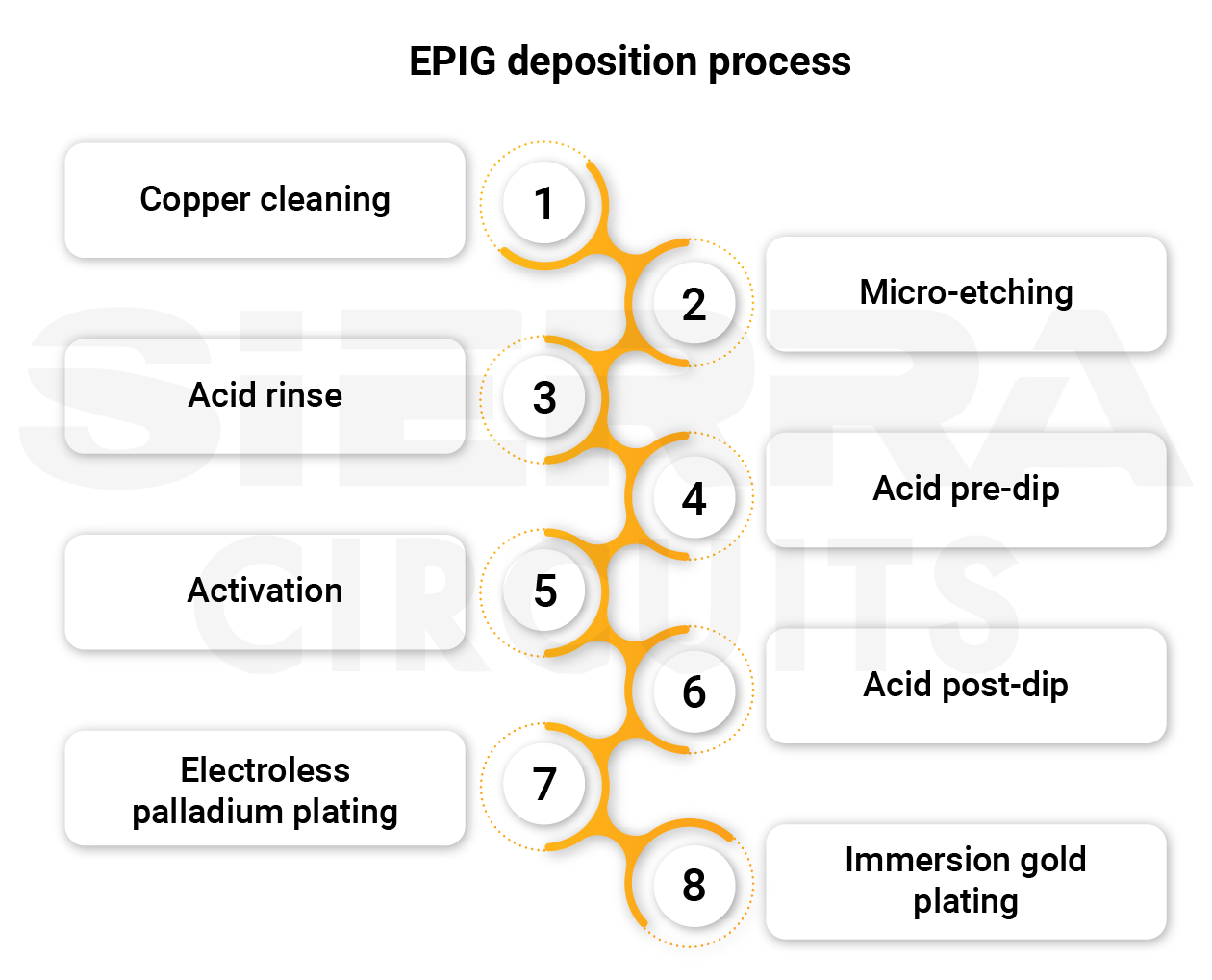
Here are the steps involved in applying EPIG coating:
Step 1: Copper cleaning
The fabricator cleans the copper surface thoroughly to remove oxides, organic contaminants, and residues. The PCB is immersed in a cleaning solution (typically an alkaline or mildly acidic cleaner), which dissolves and lifts off impurities.
This step ensures the copper is free of impurities and ready for further processing.
Step 2: Micro-etching
A mild etching solution is used to slightly roughen the copper surface. A controlled etching bath (usually a persulfate or hydrogen peroxide-based solution) removes a thin layer of copper.
This micro-etching increases surface area and provides mechanical anchoring points, enhancing the adhesion of the EPIG layers that are deposited later.
Step 3: Acid rinse
The PCB is rinsed in a dilute acid solution to neutralize alkaline residues. The manufacturer dips the board in a dilute acid bath, typically sulfuric acid, followed by water rinsing.
This prevents contamination of the PCB and helps prepare the surface for uniform processing.
Step 4: Acid pre-dip
The board is dipped in an acid solution that stabilizes the surface and adjusts the pH. An acid solution, often matched to the activation chemistry, is used to adjust surface chemistry.
This improves the wetting and uniformity of the activation layer applied in the next step.
Step 5: Activation
A palladium-based catalyst is applied to the copper surface, depositing catalytic sites that are necessary for initiating electroless palladium deposition.
Step 6: Acid post-dip
The board is treated with another acid dip to remove excess activation solution, prevent over-catalyzation, and condition the surface. This step helps control the uniformity of the palladium layer.
Step 7: Electroless palladium plating
Palladium is deposited onto the activated copper through a chemical reaction. The board is immersed in an electroless palladium bath. The chemical reaction deposits palladium without the need for an electric current.
This layer acts as a diffusion barrier and enhances corrosion resistance and solderability.
Step 8: Immersion gold plating
Displacement reaction deposits a thin gold layer over the palladium. The board is dipped into an immersion gold solution, where gold ions displace palladium atoms on the surface.
The gold layer protects the underlying palladium and copper from oxidation and provides a solderable, wire-bondable finish.
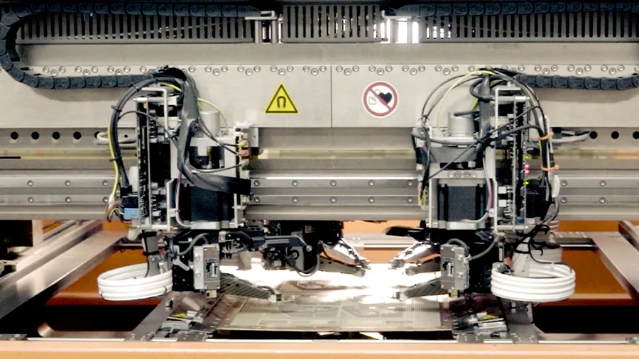
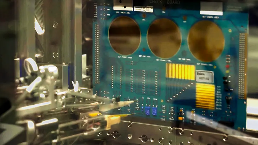
Sierra Circuits fabricates high-quality PCBs using advanced technologies such as X-ray drill machines, mechanical vision drilling systems with controlled depth, laser drilling, and Seica flying probe test machines.
Check out our rigid PCB manufacturing capabilities to learn more.
How does EPIG behave during soldering?
The gold and palladium layers of EPIG dissolve into the molten solder during reflow. As a result, the solder joint forms directly on the underlying copper surface, rather than on a nickel layer as in the ENEPIG surface finish.
This process leads to the formation of a copper-tin (Cu/Sn) intermetallic compound (IMC), in contrast to the nickel-tin (Ni/Sn) IMC found in ENEPIG coating. Based on energy-dispersive X-ray spectroscopy (EDS) analysis:
- Layer 1: A Cu₆Sn₅ intermetallic compound forms at the solder interface.
- Layer 2: A thinner Cu₃Sn layer develops adjacent to the copper base.
Why choose EPIG coating for your high-speed PCBs?
Here are 10 reasons to choose the EPIG surface finish for your circuit boards:
- Ideal for HDI PCBs
- Eliminates the bulky EN layer, allowing for finer line spacing and better routing in tightly spaced, miniaturized PCB designs.
- Enhanced signal integrity
- Without the nickel layer, EPIG avoids the skin effect, improving signal performance in high-frequency and RF PCB designs.
- The smooth, flat surface minimizes signal distortion.
- Excellent bonding compatibility
- Supports soldering and gold wire bonding, making it suitable for advanced packaging and assembly process.
- Creates solder joints directly on copper, enhancing reliability.
- Improved mechanical flexibility
- The nickel-free structure prevents cracking in flex circuits during bending, while maintaining strong solderability and bondability.
- Quicker manufacturing lead time
- EPIG surface finish speeds up fabrication compared to ENEPIG by eliminating the EN layer plating. Generally, depositing the electroless-nickel layer takes up more time during the ENEPIG surface finish process.
- Corrosion and aging resistance
- Removes nickel-related risks such as corrosion and thermal degradation, improving long-term durability in harsh environments.
- Easy to inspect and rework
- Easy to inspect visually due to its smooth, uniform finish.
- Reworkable in most cases, allowing component repair or replacement without damaging the finish.
- Thin and lightweight
- Offers a uniform, ultra-thin coating (typically 0.08–0.15 μm), ideal for space- and weight-sensitive designs.
- Environmental friendly
- RoHS compliant, free of hazardous substances.
- Strong and reliable joints
- Palladium’s hardness supports robust wire bonding.
- Produces solder joints that resist thermal stress and prevent delamination during reflow.
Limitations:
- EPIG can cost more than other finishes like hot air solder leveling (HASL) or ENIG, primarily due to the higher cost of palladium used in the process.
- While EPIG provides excellent performance, it may not be as durable as ENIG when subjected to multiple reflow cycles, making it less ideal for certain high-temperature or repeated soldering applications.
- Compared to ENIG, EPIG is not as widely available. Some PCB manufacturers may not offer it due to limited options for sourcing. At Sierra Circuits, we offer EPIG surface finish engineered for your advanced, high-frequency, and high-density PCB designs.
Also, see types of circuit board surface finishes.
What kind of applications require EPIG surface finishes?
- Medical devices and sensors: Medtech boards that go into biosensors and wearable health monitors require EPIG to avoid adverse skin reactions in sensitive patients. Nickel may cause allergy and biocompatibility concerns in sensitive patients.
- Flexible circuits: In flexible PCB designs, nickel can become brittle and crack under repeated bending or flexing, leading to circuit failure. EPIG, being nickel-free, offers better mechanical reliability in foldable smartphones or medical diagnostic strips that require repeated movement.
- Magnetically sensitive electronics: Nickel is magnetic, and its presence can interfere with the operation of devices sensitive to magnetic fields. EPIG avoids this issue entirely, hence it is the best choice for applications like GPS receivers or compasses.
- High-frequency and RF circuits: Nickel can cause signal degradation at high frequencies due to the skin effect. EPIG provides a smoother and more conductive surface required for aerospace RF boards or 5G communication devices.
EPIG is a premium PCB surface finish offering a nickel-free, wire-bondable, high-performance alternative to traditional finishes like ENIG.
Though it comes at a higher cost, its advantages in signal integrity, reliability, and suitability for high-frequency applications make it an excellent choice in advanced electronic designs.
