


Contents

On-demand webinar
How Good is My Shield? An Introduction to Transfer Impedance and Shielding Effectiveness
by Karen Burnham
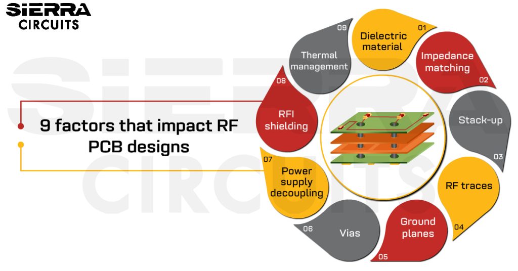
An RF PCB design is a bit different from a conventional board. It is more susceptible to signal integrity issues and performance degradation due to high-frequency operations. As an RF engineer, you must carefully consider factors such as material selection, trace layout, impedance control, and thermal management to design an efficient radio-frequency board.
In this article, you will learn 9 factors that influence your RF PCB design and the methods to resolve them.
Highlights:
Factors that impact RF board design include:
- Dielectric constant: Materials with a higher dielectric constant (Dk>4) slow down signal propagation.
- Controlled impedance: Impedance mismatch due to improper trace geometry leads to signal distortion.
- Stack-up: Poorly designed stack-ups can lead to higher EMI.
- Thermal management: Inadequate thermal management can alter the dielectric properties of the PCB material.
1. Substrates with Dk>4 increase propagation delay
RF PCBs are manufactured with certain materials that fulfill high-frequency operation requirements. These materials should have low signal losses, be stable over high-frequency operation, and be able to dissipate heat effectively.
How dielectric materials affect the RF board’s performance
Dielectric materials play a decisive role in shaping an RF board’s performance because they directly influence signal speed, loss, impedance stability, and overall electromagnetic behavior. Here are the material factors that influence high-frequency performance:
- Dielectric constant (Dk): Materials with a low dielectric constant (Dk<4) allow signals to travel faster, which is crucial for high-frequency applications. Further, a consistent dielectric constant helps maintain consistent impedance, which is critical for signal integrity. Typical values of the dielectric constant range from 3 to 3.5 for these boards.

Electric lines of force in low Dk and high Dk PCB materials. - Loss tangent (tan δ): Materials with a low loss tangent minimize signal attenuation, ensuring the signal strength remains high over long distances and reducing energy loss as heat. Loss tangent values are in the range of 0.0022 to 0.0095 for the frequency range of 10-30 GHz.
- Thermal properties: Good thermal conductivity (>0.5 W/mK) helps in effective heat dissipation, which is important for maintaining the board’s reliability under high power conditions. Select materials with a CTE close to that of copper to prevent mechanical stresses and potential failures due to thermal cycling.
- Mechanical stability: High mechanical stability ensures that the board can withstand physical stresses during manufacturing and operation. Materials with excellent dimensional stability and low CTE do not warp or deform easily and maintain consistent electrical properties.
- Moisture absorption: Materials with low moisture absorption rates prevent changes in dielectric properties, ensuring stable performance even in humid environments. Low moisture absorption also reduces the risk of corrosion and other moisture-related damage.
- Fabrication compatibility: The choice of material affects compatibility with different fabrication processes, such as lamination, drilling, plating, and surface finishes, which in turn can affect signal quality.
Apart from all these specific necessities, the material cost of manufacturing the board is also considered.
Materials made of polytetrafluoroethylene (PTFE), ceramics, and hydrocarbons mixed with one another or with a form of glass are commonly used. Rogers material is a common choice for RF circuit boards, especially for 5G PCB designs.
For more RF material selection tips, read how to pick RF PCB materials: 6 important factors to consider.
2. Impedance mismatch leads to inefficient signal transmission
In RF boards, maximum power transfer without distortion occurs when the impedance remains the same throughout the trace. This impedance is known as the characteristic impedance (Z0).


The input impedance must align with the output impedance at all frequencies to ensure the efficient operation of a circuit. To maximize performance, it is crucial to carefully match impedance levels between different components on the board, including the power supply and antenna connections. This improves the signal-to-noise ratio (SNR).

The Z0 depends on the thickness of the substrate, trace width, trace thickness, and clearance between the RF traces and ground fill. These parameters are often ignored in standard designs, but they play a major role in high-frequency RF applications.
Where exactly is impedance matching used in RF circuits?
Impedance matching is implemented at every point in an RF circuit where maximum power transfer, minimal reflection, and signal integrity are critical. You’ll find it between antennas and transmitters, at the interfaces of amplifiers and filters, along transmission lines, and anywhere components with different characteristic impedances interact.
For instance, RF energy harvesting systems use impedance-matching circuits before power rectification. Typically, this involves matching the rectifier’s (load side) and antenna’s (source side) impedances for maximum power transfer.

Generally, impedance-matching circuits are used in:
Antenna feed lines: The power amplifier’s impedance should be matched with the antenna’s to ensure maximum power transfer from the power amplifier to the antenna. For tips on antenna placement, see antenna integration and RF design guidelines for 5G PCBs.
Low-noise amplifiers: Here, impedance matching is used to achieve the lowest possible noise. The amplifier has an optimal source impedance for minimizing noise, and impedance circuits adjust the input impedance of the amplifier to match this optimal value.
Power dividers: Power dividers, such as Wilkinson power dividers, are used in RF circuits to split or combine power. Impedance matching is essential for ensuring maximum power transfer from the power divider to the load.
The most common Z0 values for RF and high-speed digital applications are 50 Ω and 75 Ω. The selection depends on the application, industry standards, and component requirements.
17 design tips for impedance matching in RF boards
- Use materials with a low dielectric constant (<4) and low loss tangent (0.0022 to 0.0095) to minimize signal attenuation and distortion.
- Adjust trace geometry by modifying the width, thickness, and clearance to achieve the desired characteristic impedance. Wider traces result in lower impedance, while narrower traces lead to higher impedance.
- Opt for thinner conductive layers to minimize signal attenuation and maintain signal integrity.
- Optimize the trace separation to reduce crosstalk between traces.
- Minimize trace lengths to reduce overall propagation delay. When necessary, adjust trace lengths to match propagation time within groups of traces.
- Address and mitigate parasitic capacitance, inductance, via effects, and pad effects. Ensure careful layout design and optimized manufacturing processes to maintain impedance consistency.
- Create matching circuits considering the geometry of the traces, including trace width, trace thickness, and height from the reference ground plane.
- Strive for tighter impedance tolerance. While the standard tolerance is +/-10% ohms, Sierra Circuits offers tighter tolerances of ±5%.
- Use simulation tools to model and analyze impedance characteristics. This helps you refine designs iteratively to achieve optimal performance.
- Implement microstrip and coplanar waveguide PCB transmission lines to route RF traces. Modify the width and thickness of these lines to achieve the intended impedance matching.
- To achieve impedance matching, use a transmission line stub, either open-circuited or short-circuited. The length and position of the stub can be adjusted to achieve the desired matching. This method is commonly employed in narrowband applications.

Intentional and unintentional stubs across an RF trace. - Refer Smith chart as a visual aid to design and analyze impedance-matching networks. It simplifies the process of identifying the necessary components and their values for achieving impedance matching by plotting the impedance of the load and source.
- Utilize the concepts of series and parallel resonance by leveraging the natural frequency properties of LC circuits to form an L, Pi, or T section impedance matching network. Carefully select inductor and capacitor values to equalize impedances at specific frequencies and place the matching network close to the component to mitigate reflections.

PI, T, and L matching network topologies. -
Use series impedance matching by positioning a series capacitor or inductor at the load end to equalize input and output impedance. Apply shunt impedance matching by connecting an inductor or capacitor in parallel at the source end.
- Conduct load-pull analysis to simulate how different load impedances affect RF transistors or amplifiers. This will help you find the optimal load impedance for maximizing power output and efficiency.
- Employ quarter-wave transformers (transmission line segments one-quarter wavelength long at a specified frequency) to change impedances and reduce reflections. This technique is ideal for RF signals operating at a single frequency or within a very narrow bandwidth.

Quarter-wave impedance transformer placement between two source and load impedances - Integrate a balun transformer to convert signals between balanced and unbalanced states. It plays a critical role when linking unbalanced RF sources to balanced antennas or vice versa. In balun transformers, this is achieved by selecting the appropriate turn ratio (ratio between primary and secondary coil inductances).

A simple balun configuration with an RF-compatible transformer
The above-mentioned impedance matching techniques have their own benefits and drawbacks. The selection of the appropriate techniques relies on the particular needs of the RF circuit and its operating frequency.
To learn how to design an RF PCB with high signal integrity, download our design guide.
RF & Microwave Design Guide
8 Chapters - 44 Pages - 60 Minute Read
What's Inside:
Download Now
3. Asymmetrical RF stack-up leads to board warping
A well-planned RF PCB stack-up design is crucial in ensuring structural integrity and signal integrity, reducing crosstalk, and mitigating EMI within high-frequency analog designs.
The radio-frequency components and traces are placed on the top layer. This layer is immediately followed by a ground plane and a power plane. All the non-RF components and traces are populated on the bottom layer.

This arrangement offers minimum interference between RF and non-RF components. The immediate ground plane provides a minimum path for the ground return current. This is an example stack-up suitable for small radio-frequency boards.
4 best practices to design RF PCB stack-up
The arrangement of dielectric, foil, and core materials in a printed board is known as the layer stack-up. It is crucial to optimize the stack-up for RF designs in order to achieve effective isolation, shielding, and impedance control. Key considerations for RF stack-up configuration include:
- Maintain proper layer sequencing and isolation
- Space power and ground plane layers across the stack-up; these layers serve as protection to reduce EMI and offer consistent voltage references. Power and ground planes are placed as adjacent internal layers.
- Place signal layers between ground planes in an alternating pattern to minimize signal interference and maintain consistent impedance in the transmission lines.
- Position components on the surface layers, as they provide space for soldering various electronic components.
- Maintain stack-up symmetry by strategically placing copper planes (ground and power) on opposite sides of the core. This promotes thermal stability by allowing uniform expansion and contraction during temperature changes.
- Choose foil thickness based on your application
- Standard RF PCBs use copper foils that are usually between 1/2 oz and 2 oz thick. However, the ideal thickness depends on the specific application.
- Employ thicker copper for power planes because of its capacity to manage higher currents.
- Utilize different foil shapes, such as trapezoidal or tapered profiles, in some radio frequency applications to achieve more precise management of trace impedance, which is crucial for higher frequencies.
- Choose smoother copper foils with lower surface roughness for RF PCBs. Rougher copper surfaces can lead to increased signal loss at higher frequencies.

- Optimize core thickness in RF boards to ensure proper signal integrity
- Prefer thinner cores as they enable finer lines and gaps on copper layers, which is advantageous for high-frequency circuits needing smaller features. Additionally, thinner cores can achieve the same functionality with fewer layers, reducing fabrication complexity and cost.
- Opt for thermally conductive core materials for applications that generate significant heat. These cores aid in heat dissipation throughout the PCB, preventing overheating and potential component damage.
- Choose an optimum number of layers
- Avoid using 2-layer stack-ups for RF circuit boards due to insufficient clearance for high-frequency applications. However, they may be used for cost-saving and simpler designs in lower frequency ranges (kHz).

The top layer should include all the RF components, decoupling capacitors, traces, etc., and try to provide an individual layer for the ground.
-
- Prefer using 4-layer stack-ups over 2-layer for RF PCBs to provide dedicated ground and power planes, with RF signals and components arranged in outer layers and the ground and power planes as inner layers.

-
- Consider higher layer counts for greater routing flexibility in complex designs, but be aware that they result in a thicker PCB and potentially higher costs. Determine the optimal layer count based on specific design requirements. A range of 6 to 12 layers is common for RF PCBs, offering a good balance.
Read how the modular PCB design method simplifies complex layouts to reduce errors and rework of your circuit designs.
By carefully considering these key factors during the stack-up design process, you can create an optimized RF PCB that ensures signal integrity. However, any layer misalignment during fabrication can lead to impedance mismatches and signal integrity problems, affecting the performance of high-frequency RF circuits.
At Sierra Circuits, we control curing parameters like temperature, pressure, and time to minimize inherent and residual stress, thus eliminating the risk of layer misalignment. Visit our RF and microwave PCB capabilities to learn more.
4. Narrow RF traces increase heat generation
RF traces propagate high-frequency signals and are thus subject to transmission losses and interference issues. The characteristic impedance of these traces is a main concern among RF PCB designers.
In radio-frequency boards, the traces are regarded as transmission lines. The most common types of RF transmission lines designed are coplanar waveguides (CPWG) and microstrips.
Coplanar waveguides operate in a quasi-TEM mode, where a negligible portion of the EM field extends outward. This provides low dispersion and minimal dielectric loss, maintaining strong signal quality across a broad frequency range, making it a preferable choice for microwave boards.
To learn more about the benefits of using CPW for high-frequency applications, see microwave PCB material selection and CPW for signal integrity.
Why place RF signals on the outer layers of a board?
RF signals are typically routed on the outer layers because they need a clean, controlled environment to maintain signal integrity at high frequencies. The outer layers provide a direct reference plane, lower loss compared to traveling through dielectric material, easier impedance control, and reduced via transitions that can introduce component parasitics.
Here are other reasons to consider:
1. Speed of electromagnetic waves: The speed of electromagnetic waves is highest in the outer layers because the effective dielectric constant is lowest. On the outer layers, the presence of air, which has a very low dielectric constant, further reduces the effective dielectric constant, increasing the signal speed.
2. Hybrid stack-up considerations: In a hybrid stack-up, materials between layers 1 and 2 are usually high-frequency materials like Rogers, which have low dielectric constants (around 2 to 3). This results in higher signal speeds on the outer layers.
3. Propagation time: Reducing propagation time is crucial in high-frequency applications, and the higher signal speed on the outer layers helps achieve this.
4. Core construction stability: A core construction is often used between layers 1 and 2 in high-frequency RF traces. The core’s thickness remains constant regardless of copper percentage, providing a stable dielectric thickness and dielectric constant. This stability leads to better control over the impedance, making it advantageous to route RF signals on the outer layers.
11 radio frequency trace design aspects
- Route RF traces first, and it is essential to employ impedance-matching techniques for each RF trace.
- Utilize microstrips for RF traces to handle short interconnections between components, ideally within a shielded area with outer metal layers.

A microstrip line on an RF printed board allows for a compact layout - Keep the length of RF traces as short as possible to reduce attenuation.
- Avoid placing RF traces parallel to signal traces to prevent interference.
- Include ground planes to provide return paths for signals. Fill the area around RF traces with ground and ground vias to connect with inner ground layers for better isolation.
- Route traces directly to vias whenever possible to minimize stubs. This helps maintain signal integrity and reduces the risk of signal reflections and crosstalk.
- Use wider traces to reduce resistance and inductance, minimizing signal loss. However, wider traces can increase the risk of crosstalk and interference, so a balance is necessary based on the specific RF circuit requirements.
- Evaluate whether to remove the solder mask from RF traces based on assembly and electrical performance considerations. Note that solder mask design rules typically specify a 4 mil spacing between the solder mask edge and the trace edge.
- Remove the solder mask from RF traces for extremely low-loss and very high-frequency applications to prevent increased loss from the solder mask’s higher dielectric constant.
- Avoid placing test points on RF traces. Doing so will interrupt the trace’s impedance-matching values.

Avoid placing test points on RF traces - Miter right-angled traces to ensure constant impedance across the bends. The mitering of a trace is shown below:

Here, M is given by the following formula:
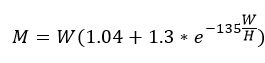
where,
M- mitering width
W- RF trace width
H- substrate height

5. Inadequate RF ground planes increase interference
Any radio-frequency trace or component requires a return path for the current propagating through it. A ground plane takes care of this. One of the first questions when designing ground planes is what grounding strategy you will be using.
RF/high-frequency boards typically employ a multi-ground approach, in which all ground connections on the board are linked by a single plane through low-impedance connections. This technique of shortened connections helps to minimize EMI that may occur at higher frequencies.
11 ground plane design considerations for RF PCBs
- Include a dedicated ground plane for each RF layer. This ground plane is placed immediately below the layer to make the current flow path the shortest.

- Design a continuous ground plane with no breaks. Breaks in the ground plane can force return currents to take longer paths, increasing inductance and potentially causing signal integrity issues.
- If you’re adding a partial ground plane, make sure it underlies all RF components and transmission lines.
- Add ground vias liberally throughout the RF section to minimize parasitic inductance caused by ground-current return paths. These vias also help prevent cross-coupling between RF and other signal lines.
- Provide return ground paths for each RF component and trace, with a consistent ground plane for each RF signal layer.
- Fill the space between shield cavities and the RF section outline with as much ground as possible to improve shielding effectiveness.
- Connect each ground pin or via to the ground plane separately. Avoid daisy chain connections to the ground pins, as this can increase the return current loop.
- Implement top and bottom ground pours in RF PCB layouts to mitigate EMI, reduce crosstalk, and enhance controlled impedance while ensuring continuous low-impedance return paths.
- Ensure that ground pours do not create isolated ground islands, which can act as unintended antennas or cause ground loops. Instead, use vias or copper bridges to connect any isolated ground areas back to the main ground plane.
- Maintain appropriate clearance between signal traces and ground pours to avoid short circuits and ensure manufacturability.
- Keep sufficient clearance around component pads to prevent solder bridging during assembly.
- Use a solid ground fill pattern rather than a hatched pattern, as it provides better shielding and lower impedance.
- Make sure that the vias connecting the ground pours have appropriate thermal relief patterns to facilitate effective soldering and heat dissipation.
- Utilize the maximum number of vias for transitioning from the ground fills on the top layer to the inner ground layers.
The via stitching gap choice between λ/20 and λ/10 depends on the specific value of λ. If the λ value is too small to accommodate λ/20, then λ/10 can be used. Ultimately, the preferred spacing between vias should be determined based on calculations and considerations of the specific application.
| Frequency | Wavelength | 1/20th wavelength |
|---|---|---|
| 2.5 GHz | 12 cm | 6 mm |
| 3.0 GHz | 10 cm | 5 mm |
| 4.0 GHz | 7.5 cm | 3.75 mm |
| 5.0 GHz | 6 cm | 3 mm |
- Use at least two grounding vias for each shunt-connected component, such as power-supply decoupling capacitors, to reduce the effect of via parasitic inductance. Implement via ground islands for groups of shunt-connected components.
- Ensure a solid ground plane on the component layer (top or bottom of PCB) underneath the IC to carry DC and RF return currents. This component ground paddle also acts as a thermal heatsink. The paddle, preferably plated and filled with thermally conductive paste, should include the maximum number of through-vias allowed by design rules.

6. Vias induce parasitic capacitance in RF boards
The electrical performance of a PCB can be greatly affected by the size, shape, and location of vias. Via design plays a crucial role in establishing the impedance of a trace.
A via induces parasitic capacitance in a circuit board. In the case of radio-frequency boards, this capacitance affects the high-frequency operation. Therefore, to reduce the parasitic capacitance and interference at these frequencies, specific via diameters and lengths must be followed.
11 tips to keep in mind when designing vias for RF PCBs
- Restrict the use of vias to route an RF trace from one layer to another. In cases where vias cannot be avoided, it is recommended to position ground vias near signal vias.
- Introduce more parallel vias to reduce the parasitic inductance.
- Utilize dedicated vias for each pin of a component.
- To reduce parasitic inductance in RF PCB designs, minimize the diameter of vias, aiming for typical diameters within the range of 0.2 mm (8 mils) to 0.4 mm (16 mils) or smaller.
- Use vias to form ground shielding around the RF section whenever possible.
- Implement ground plane via stitching wherever applicable. This establishes a shorter ground return path for the current.
- Use the maximum number of vias between the top layer ground plane and inner layer planes as allowed by the design. These vias should be placed at a distance not exceeding 1/20th of the signal wavelength.
- Space vias farther apart to decrease their impedance, as fewer vias in a given area result in lower impedance compared to densely packed vias in close proximity to each other.
- Place vias evenly along both sides of the transmission line to isolate noise from nearby traces or ground layers.
- Consider the circuit’s current requirement, mechanical stress, and its resilience to thermal expansion when choosing the ideal via depth. The via impedance increases with its depth due to the increased capacitance between two planes. A shallower via has less capacitance but is more prone to cracking during reflow soldering.
- Use a lower aspect ratio for optimal signal performance. Higher aspect ratios can increase inductance and negatively impact signal performance. In RF PCBs, a typical aspect ratio might range from 0.8 to 1.2.
For more via design tips for radio frequency boards, see 4 RF PCB via design challenges with layout solutions.
7. Inefficient power supply decoupling increases noise
Noise reduction is extremely critical when it comes to radio-frequency boards. At high operating frequencies, these boards become very sensitive to the effects of noise. Therefore, all possible methods are employed for noise removal. One such method is called power supply decoupling.
This process filters noise carried into the circuit through the power supply. The capacitors designated for this are called decoupling capacitors. These capacitors are connected across the power supply.
Impedance matching is an integral feature of every RF circuit board. Hence, after the connection of decoupling capacitors, the impedance of the whole circuit should not change. Further, the placement of decoupling capacitors is also an important part of getting the RF design right.
7 strategies to place decoupling capacitors on RF circuit boards
- Always connect capacitors with minimum impedance for efficient decoupling.
- Operate the capacitors at the self-resonant frequency (SRF) to yield minimum impedance. A capacitor’s SRF is inversely proportional to its capacitance value.
- Choose capacitors whose SRF is close to the noise frequency.
- When using multiple decaps, place the smallest-value capacitor closest to the power supply pin, as shown below. The higher-valued capacitor is meant to filter low-frequency noise in the system and store energy, while the lower-valued capacitor filters out high-frequency noise.

Place the smallest valued capacitor nearest to the power pin in RF PCB designs - Position the decoupling capacitors on the same layer as the components.
- Arrange the capacitors in parallel to the signal flow path.
- Employ individual ground vias for each capacitor. Never share ground vias.
For more on decaps, read decoupling capacitor placement guidelines for PCB design.
8. Poor shielding increases RF interference
Electromagnetic interference caused by radio waves is known as radio frequency interference (RFI). High-frequency signals are more susceptible to interference from external EMI and crosstalk from nearby traces.
Safeguarding electronic devices from RFI is crucial to maintain their optimal performance. Shielding is a viable approach to prevent RFI.
8 strategies to prevent unwanted RF interference
- Shield individual traces that carry high-frequency signals and utilize shielded connectors to help reduce signal leakage and interference. Further, ground the shields to provide a path of low impedance for any unwanted currents.
- Use RF shields made of conductive or magnetic materials to block unwanted radio-frequency electromagnetic signals. These shields prevent frequency interference between nearby components and traces, becoming crucial for high-frequency components.
- Isolate critical circuit blocks to prevent RF regions operating at different frequencies from interfering with each other in mixed-signal systems. This ensures analog signals do not interfere with digital signals.
- Maintain proper isolation between components and traces to minimize interference and crosstalk between neighboring circuits and to separate analog and digital signals.
- Strategically position isolation materials or ground planes between active layers to prevent signal leakage and interference.
- Optimize component placement in various layers, taking into account their functions and connectivity needs to maximize signal efficiency.
- Keep noisy components away from sensitive signal paths, which often require meticulous layout planning.
- Separate RF transmission lines from other traces, especially high-speed signals. Route high-speed signals on a different layer than RF signals.
- Isolate high-power signals from other circuit parts. Power supply lines should be routed on dedicated layers with suitable decoupling/bypass capacitors.
- Utilize via fencing, a popular and cost-effective technique for spatial isolation, to shield microstrip and stripline transmission lines, provide fencing around circuit board edges, and separate different functional units on the same board. This method, applied in contemporary circuit boards for isolating BLE and Wi-Fi units, also prevents parasitic coupling between closely spaced traces by forming a via fence.

Via fencing in microstrip lines - Employ via fences on both substrates above and below the RF trace in stripline transmission lines, grounding these vias through the respective top and bottom ground planes.
- Connect via fencing in the top layer of microstrip lines with a metal track, as the top side lacks a ground plane.
- Use X-Y axis isolation to ensure maximum isolation between different circuit types in mixed-signal layouts. However, note that it requires a slot in the stack-up, which can interrupt the ground plane’s continuity. To avoid this, provide a bridge area to route the circuitry from one part of the board to another, ensuring the continuity of planes and circuits.

Some of the important design aspects for X-Y isolation are:
-
- Create the slot as either a physical cut-out or a copper layer slot.
- Connect the RF layer and digital layer grounds through the bridge.
- Form the bridge on a ground plane at a specific location.
- Design the slot as a no-go zone, except for the ground layers, which need to remain continuous.
- Utilize this method of spatial isolation effectively when digital signals do not penetrate significantly into the RF zones of the PCB design.
- Divide the digital and analog routing into two separate zones.
- Use RF gaskets and seals around enclosures or connectors to improve the ability to block electromagnetic interference. Close gaps and seams with these components to reduce the risk of electromagnetic leakage.
- Beryllium copper (BeCu) and metalized fabric gaskets are preferred gasket choices when designing microwave PCBs.
- Employ an RF can as a shielding device to block electromagnetic interference in a circuit. It functions like a metal cover that surrounds components emitting RF interference. This shielding mechanism decreases the transmission of magnetic and electric radiation from the source area to other vulnerable sections.
- Use Faraday cages to shield important RF components or entire sections of RF microwave PCBs from external electromagnetic interference. These cages, typically constructed from conductive materials such as copper, act as barriers to block unwanted signals from entering sensitive areas.

Faraday’s cage to shield critical RF components - Design RF chokes as inductors specifically to block or attenuate high-frequency AC signals while allowing DC or lower-frequency AC signals to pass. They prevent the egress and ingress of unwanted RF signals in a circuit.
Best practices for using RF chokes in RF PCB layout
-
- Place RF chokes as close as possible to the source of the unwanted signal or noise to effectively filter it out before it can spread.
- Ensure a continuous, solid ground plane under the RF choke to minimize ground loop issues and provide a low-impedance path for return currents.
- Keep the connections to and from the RF choke as short and direct as possible to minimize parasitic inductance and capacitance.
- Maintain controlled impedance in the traces leading to and from the RF choke to avoid signal reflection and loss.
- Choose RF chokes that are effective over the frequency range of your application. The choke should provide high impedance at the frequencies you want to filter out.
- Ensure the RF choke can handle the maximum current expected in the circuit without saturation or significant loss.
- Use decoupling capacitors in conjunction with RF chokes to filter out high-frequency noise. Place these capacitors close to the power pins of sensitive components.
- Consider using Pi (π) or T filters, which combine RF chokes and capacitors, for more effective noise suppression.
- Ensure that the RF choke can dissipate heat effectively. Use thermal vias and pads if necessary to manage heat.
- Keep RF traces and chokes away from high-speed digital signals and other noisy traces to minimize interference.
For more high-speed circuit board design tips, download our eBook.

High-Speed PCB Design Guide
8 Chapters - 115 Pages - 150 Minute ReadWhat's Inside:
- Explanations of signal integrity issues
- Understanding transmission lines and controlled impedance
- Selection process of high-speed PCB materials
- High-speed layout guidelines
Download Now
9. Inefficient thermal management alters the dielectric properties of RF PCBs
High temperatures pose significant challenges in RF boards. Elevated temperatures can alter the dielectric properties of the PCB material, affecting signal propagation and phase stability.
Excessive heat reduces the lifespan of RF components, leading to premature failures and increased maintenance costs. Additionally, temperature-induced variations can cause frequency drift in RF circuits, impacting their ability to maintain accurate and stable frequencies.
20 thermal management techniques for RF PCB designs
- Add plated through holes (PTHs) to thermal/ground pads under components to dissipate heat to a thermal sink, such as a cold wall.
-
- Make sure to pre-fill these PTHs to prevent solder wicking. Mitigate the risk of poor or unreliable connections by ensuring proper solder filling in the PTHs.
- Utilize proprietary via plugging paste to fill PTHs under components and plate over the top to create an uninterrupted ground pad.

Comparison of total thermal conductance of filled vias - Apply electrically and thermally conductive paste, such as silver (Ag) loaded epoxy, to fill the thermal PTHs. Note that even with Ag epoxy, the thermal conductivity of these pastes typically ranges from 4 to 30 W/mK, which remains relatively low.
- To improve thermal conductivity, increase the plated wall thickness of PTHs from the standard 25 µm to 100 µm.
- Utilize a greater number of smaller PTHs within a ground pad to create a more effective thermal path compared to fewer larger PTHs.
- For applications where heat transfer is critical, use a through-hole wall thickness of 0.1 mm. For standard applications, you can use the standard 0.025 mm.
- Integrate copper coins into the circuit’s structure. A more common method involves stepping the coin to ensure that heat is not only efficiently conducted away but also evenly distributed.

- Use metal-backed circuits to efficiently dissipate large amounts of thermal energy. Opt for metal backings such as copper, aluminum, or brass, which are commonly used in solid-state power amplifiers (SSPA). These circuits can be constructed as either pre-bonded or post-bonded structures.
- Pre-bonded circuits come with a thick metal backing, which limits trace design to a single layer and complicates processing due to required post-trace machining. Despite the risk of damaging critical features, this approach offers an excellent ground plane reference.
- Post-bonded circuits are easier to manufacture as the circuit is created and verified before being attached to a pre-machined, plated metal backing. This method allows for multiple conductor layers and typically uses a conductive adhesive for bonding.
- Mount components that need heat transfer directly onto the metal backing through openings in the circuit for both pre-bonded and post-bonded circuits.
- Employ metal-core stack-ups to address space constraints and achieve high isolation between RF and control circuits. Transfer heat from components to the core either through thermal vias or by direct contact via cavities within the circuit where components are mounted.
- Consideration must be given to removing heat from the core. Typically circuit substrate is machined away from two edges to expose the core and can be clamped within the chassis to transfer heat.
- In the case of thermal vias where holes are blind with diameters <0.2mm and depths <0.3 mm, the holes can be filled with copper using a blind hole plating process.
- Utilize wide bandgap materials like gallium nitride (GaN) and silicon carbide (SiC) to create high-power-density devices that operate efficiently at high frequencies and temperatures with minimal power losses.
- Advanced materials, such as metalized synthetic diamond and aluminum diamond metal-matrix-composite (MMC), offer extremely high thermal conductivity (500 W/mK or more) for effective heat dissipation from GaN and other high-power semiconductors.
- Use chemical vapour deposition (CVD) diamond heat spreaders to achieve lower operating temperatures and simplify the overall thermal management solution.
- Leverage diamond’s high thermal conductivity (up to 2000 W/mK, five times greater than copper) for superior performance in thermal management, especially where electrical isolation is required.
- Use heat sinks, typically made of thermally conductive materials like aluminum or copper, to increase surface area for heat dissipation.

Heat dissipation from hotspots to the heat sink. - Incorporate thermal vias and thermal planes (solid copper planes) in the PCB stack-up to facilitate heat transfer and spreading.
- Apply thermal interface materials (TIMs) between heat-generating components and heat sinks or cooling surfaces.

-
- Use thermal interface material, such as thermal grease, insulators with conductive particles mixed into the elastomer, Panasonic’s diamond films, and heat control products offered by Bergquist, can be used between the heat sink and the components to ensure efficient thermal contact.
- Use forced air cooling by employing fans or blowers to circulate air over the PCB and heat-producing components, improving convective heat transfer. This method is suitable for systems where passive cooling is inadequate or additional cooling capacity is required.

- Implement liquid cooling systems with coolants such as water or specialized fluids to directly dissipate heat from components or PCBs. While these systems are highly efficient, they can introduce additional complexity and cost to the design.
- Incorporate thermoelectric coolers (TECs), which are solid-state devices utilizing the Peltier effect to actively move heat from one side of the device to the other. TECs are effective for localized cooling of specific components or hotspots on the PCB.
- Use substrates with high thermal conductivity, such as aluminum nitride (AlN) or ceramic-based materials, to enhance heat dissipation compared to traditional FR-4 substrates. These materials are particularly beneficial for high-power or high-frequency applications.
- Employ dielectric materials with improved thermal properties, like woven glass-reinforced hydrocarbon/ ceramic laminates, to enhance heat spreading and dissipation while preserving electrical performance.
- Increase the thickness of copper layers or add extra copper planes within the PCB stack-up to boost heat spreading and dissipation capabilities.
- Use computational fluid dynamics (CFD) and finite element analysis (FEA) tools to model and analyze thermal behavior. These thermal simulation tools help designers identify potential hotspots, optimize component placement, and assess the effectiveness of various cooling strategies.
By incorporating thermal simulations early in the design process, engineers can make informed decisions regarding material selection, placement of PCB components, heat sink design, and overall thermal management strategies. Iterative design optimization cycles can be performed to achieve the desired thermal performance while considering other design constraints, such as size, weight, and cost.
Key takeaways
- Match impedance across components (e.g., antennas, amplifiers) to maximize power transfer and reduce noise.
- Select materials with low-loss tangents to minimize signal attenuation and good thermal properties for heat dissipation.
- Ensure proper isolation between RF and non-RF components, and use dedicated layers for power and ground planes.
- Maintain stack-up symmetry and optimize foil types and core thickness to support high-frequency operations.
- Implement microstrip and coplanar waveguide transmission lines and consider using quarter-wave transformers and baluns as needed.
- Use ground planes to provide return paths and minimize interference. Avoid isolated ground islands.
- Consider removing the solder mask for very high-frequency applications to minimize losses.
- Use mitering for unavoidable sharp bends to maintain impedance.
- Avoid breaks in ground planes to maintain low-impedance return paths.
- Add ground vias liberally to minimize parasitic inductance and enhance isolation.
- Place decoupling capacitors as close as possible to power pins and use capacitors with appropriate self-resonant frequencies.
- Employ shielding techniques like RF shields, via fencing, and Faraday cages to block or reduce interference.
- Use techniques like plated through holes, copper coins, metal-backed circuits, and advanced materials to manage heat effectively.
The design and fabrication of RF PCBs require more attention from both designers and manufacturers. The DFM team should strictly follow the design checklist. Since these boards are prone to interference and high-frequency noises, even the slightest mistake will affect the operation.
All of the above methods and aspects will help us to get better with the design.
See our case study on the design of an RF board with sensors to learn how we analyze your design before we fabricate your radio frequency board.
Need assistance in designing your RF and microwave PCB layout? Post your queries on our PCB forum, SierraConnect, and have them answered by our experts.

About Pooja Mitra : Pooja Mitra is an electronics and communication engineer. With an experience of over three years in the PCB industry, she creates industry-focused articles that help electrical and PCB layout engineers.


Start the discussion at sierraconnect.protoexpress.com