


Contents
Designing a PCB layout involves translating a validated schematic into a physical board by defining the stack-up, placing components, routing connections, and creating production files using CAD software.
A clear understanding of each design stage is essential for a PCB designer to ensure electrical correctness, manufacturability, and long-term reliability of the board, especially in complex and high-speed designs.
Highlights:
When designing a PCB:
- Begin with schematic capture and logical net definition.
- Validate the BOM, stack-up, and component availability during the pre-layout stage.
- Convert schematics into physical placement, routing, and planes in the PCB layout stage.
- Generate production files to ensure accurate fabrication, assembly, and verification.
In this article, you’ll learn the complete PCB design workflow, key tasks at each stage, and best practices to ensure error-free layouts using modern CAD tools.
Overview of PCB design
The first step is to draw your concept block diagram on paper. It is then developed into schematic designs using a PCB layout tool. A schematic consists of component symbols and net connections between the symbols. These nets will become traces on the circuit board.
The next phase is the pre-layout stage; in this step, the BOM from the schematic is validated for long lead time components and obsolete components. During the validation process, the manufacturing part numbers (MPN) and vendor part numbers are verified. The stack-up is also created now.
The PCB layout stage is next. In this stage, the board parameter settings, board outline, component placement, routing, and production document generation are completed.
To become a successful PCB designer, it is essential to have a solid grasp of the steps involved in designing a circuit board layout.
What are the basic steps of PCB design?
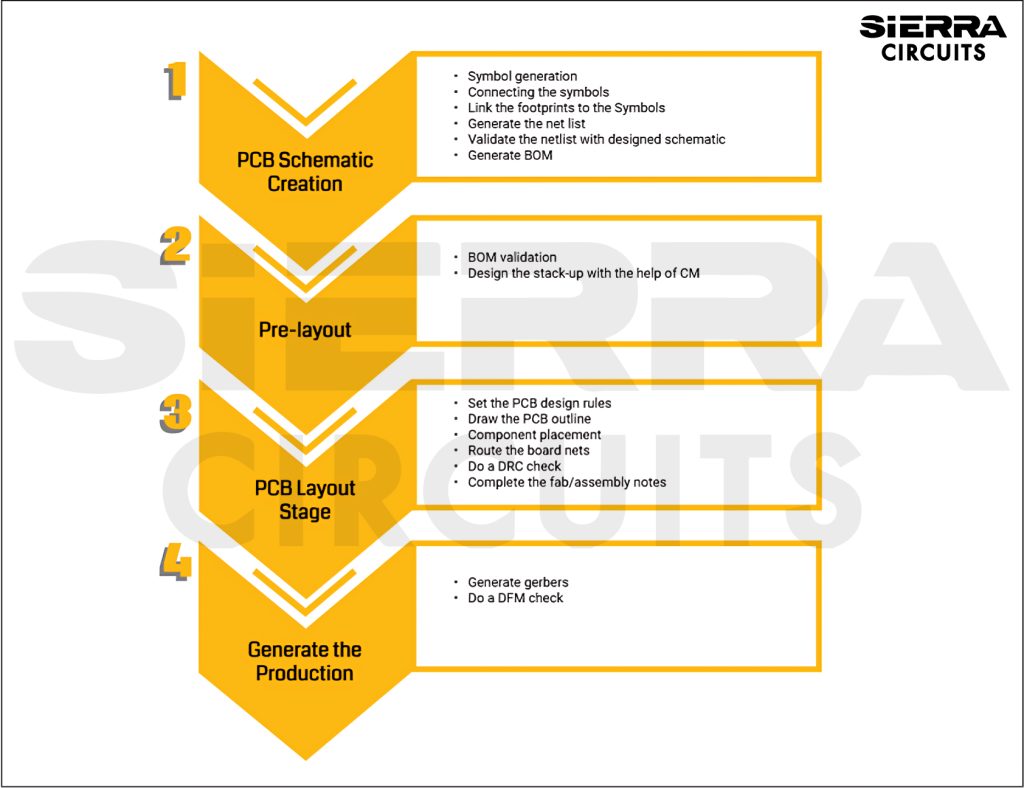
The design process involves schematic creation, pre-layout preparation, layout, and generation of production files.
Each stage has its own defined processes and checklists. To design a successful PCB, it is essential to follow the processes and check through the design checklist at every milestone. In this section, we will go through the different steps in designing a PCB using Altium Designer.
Step 1: PCB schematic creation
A schematic diagram is a representation of the elements of a system using abstract and graphic symbols.
In this phase, the design is entered into the schematic tool (Altium Designer, Cadence Allegro, Zuken CADSTAR, etc). A schematic shows the components used in the design and how they are connected.
In a hierarchical schematic, multiple functional blocks are interconnected, defining how groups of components relate across the design. An example is shown below.

To learn more about the step-by-step approach to schematic generation, refer to our post on schematic and netlist checks to ensure error-free designs.
Below are the steps involved in PCB schematic creation using Altium Designer:
1.1. Generate schematic symbol
In Altium Designer, you can access the symbol generation tool by navigating through Tools → Symbol Wizard in the main menu. The symbol creation process involves drawing the component body, adding pins and pin numbers, defining the reference designators, and assigning a footprint.
To learn more about schematic symbols and diagrams, read our article what’s the meaning of a schematic diagram?
1.2. Place schematic symbols
Symbol bodies are created using graphical objects in the schematic library editor. Altium Designer provides predefined closed shapes such as rectangles, pentagons, ellipses, and triangles.
1.3. Assign pin numbers
Pins define the connection points on the component for the incoming and outgoing signals. Pin numbering is made to ensure the connections shown in the schematic end up connected properly by copper on the PCB.
It is the component pins that give the component its electrical properties and define connection points on the component for directing signals in and out. A pin is placed to represent each pin on the actual physical component.

Pins can be placed in a schematic library document using one of the following steps:
- Click Place→ Pin in the main menu
- A Symbol Options dialog will appear. Use this dialog to define the symbol height and width, the length of its pins, and a style for its pins about the ports on the source sheet, and click OK.
1.4. Add reference designators
Reference designators mainly include category, value, manufacturer, manufacturer part number, and supplier.
Every symbol on your circuit should have its unique designator so that every part is easily identifiable. For example, every resistor should follow a consistent naming sequence of R1, R2, R3, etc.
1.5. Assign a footprint
The footprint gives an idea of the actual size of the component. For example, when we put a component on the sand, it will leave its impression there.
This imprint is its actual physical size. Some components come in standard packages, and the footprints are easy to find. In some cases, we may have to create the footprint manually.
Below are the steps to create a footprint in Altium Designer:
- Create the pads
- Key in the component height and area
- Provide the silk-screen information
- Save the footprint
1.6. Connect the symbols
It is very important for a PCB designer to clearly show how the components are interconnected in the schematic.
First, whenever you have two wires that form a junction and share an electrical connection, that intersection needs to have a junction dot. This is standard practice in every schematic design.

Schematic connections: good practice

If you have a pair of intersecting wires that are not electrically connected and are just overlapping, then you will not need a dot.

The important signals on the board should be marked once the components are connected. This marking includes impedance traces such as 50Ω SE and 100Ω differential pairs. Also, the power traces need to be identified and marked.
1.7. Link the footprints to the symbols
The component footprints are shown on the schematic diagram when you transfer the schematic information to the PCB layout.
1.8. Generate the netlist
A netlist in any PCB designing software contains information on the component name and the pad of that component that is connected. Netlist also assigns numbers to the connections in serial order.
The Netlist Manager dialog is used to control and manage the netlist of the board. Nets can be edited, added, or deleted as the requirements. The pins (or pads) of the components in the nets can also be edited.
1.9. Perform a netlist check
The export netlist option is used to export the netlist of the PCB to the current document. Once the command is launched, a netlist document with an extension ‘.Net’ is saved in the same folder where the circuit board design document is saved.
A net-by-net verification in the schematic should be carried out (whether all the nets are connected as intended).
1.10. Generate the BOM
The bill of materials (BOM) is simply a list of required materials for manufacturing a printed circuit board. In Altium Designer, a BOM can be generated by choosing the options Report → Bill of Materials from the PCB schematic.
It is always recommended to carry out a PCB layout review after every step/ sub-step to ensure an error-free design.

Design for Manufacturing Handbook
11 Chapters - 96 Pages - 90 Minute ReadWhat's Inside:
- Annular rings: avoid drill breakouts
- Vias: optimize your design
- Trace width and space: follow the best practices
- Solder mask and silkscreen: get the must-knows
Download Now
Step 2: Pre-layout stage
In the pre-layout stage, we initiate the design of the stack-up, ensure that the BOM is verified for all parts, and verify that the parts are active and not obsolete.
2.1. Validate the BOM
The BOM is simply a list of required PCB materials for manufacturing a printed circuit board. The first step in the pre-layout stage is to ensure that all the materials required for your design are available.
During the BOM validation, you need to check if:
- Manufacturing part numbers (MPN) are correct
- Vendor part numbers (VPN) are correct
- The quantity of the parts is correct
- Designators match the schematic
- DNI (do not install) components are marked in the BOM
2.2 Design the stack-up with the help of a contract manufacturer (CM)
Designers need to have the details of the stack-up before starting the layout design. You can also get help your fabricator to ensure a manufacturabale buil-up.

Step 3: PCB layout stage
The PCB layout stage includes setting up the design tool, board outline, netlist import, component placement, routing, silkscreen cleanup, DRC check, and generating documents for production (Gerbers, netlist, etc.).
3.1. Design the stack-up
The board layout starts by setting the stack-up and design rules.
Steps to design your PCB stack-up in Altium Designer:
- A single-layer stack-up, by default, is defined when a new board is created.
- The currently selected stack is duplicated if you click the Add Stack button. Once the new stack is added, the name and the properties can be changed in the stack properties tab of the dialog box.
- Click the Add Layer button for a separate solder mask and over layers.
- The order of the stack-up can be changed using the Move Left and Move Right buttons that are present at the bottom right of the stack-up tab.
- For flexible PCBs, the flex stack-up should have its Flex option enabled. Flex bending is defined by placing a Bending Line across the flex region (Design » Board Shape menu)
The image below shows the Layer Stackup Manager tool.


Controlled Impedance Design Guide
6 Chapters - 56 Pages - 60 Minute ReadWhat's Inside:
- Understanding why controlled impedance is necessary
- Stack-up design guidelines
- How to design for impedance
- Common mistakes to avoid
Download Now
3.2. Set the design rules
Design rules are instructions for the PCB layout tool to follow. Every aspect of the design is covered in the PCB constraint settings. PCB design rules can be broadly classified as:
- Electrical design rules: Deal with electrical characteristics such as impedance, frequency, etc.
- Physical design rules: Associated with parameters like trace width, via sizes, differential pairs, etc.
- Spacing design rules: Deal with spacing between power tracks of high voltage, clearance, or a particular region if we need a 5-mil tracing, etc.
These rules are defined under the PCB rules and constraints Editor Dialog box.
Also, see PCB layout rules every designer should follow to eliminate layout errors before fabrication.
3.3. Draw the PCB outline
The shape of the PCB is referred to as the board outline and is essentially a closed contour. The board shape can be redefined in different ways:
- Manually: By moving the existing board vertices. This can be done by switching to board planning mode (View → Board Planning Mode) in the design menu.
- From selected objects: This is typically done on a mechanical layer if you have the outline of the board imported from an MCAD tool (DWG/DXF file). Switch to 2D layout mode (View → 2D layout Mode), select the primitives on the mechanical layer (Edit → Select → All on Layer), then use the Design → Board Shape → Define from selected objects command.
- From a 3D body: Use this option if the blank board has been imported from a CAD tool into a 3D body object (Place → 3D Body). Switch to 3D layout Mode (View → 3D Layout Mode), then use the command in the Design → board shape sub-menu to select the board shape.
3.4. Place components in your layout
The first step of component placement begins by breaking down the layout into different sections based on the circuit’s functionality (analog, digital, high speed, high current, power supply, etc)

3.5. Enable cross-select mode
Cross-select mode enables the corresponding selection of the object between the PCB layout and the schematic. In other words, if you select an object on the layout, the corresponding object on the schematic is also selected. This ensures accurate component placement on your layout.
The image below shows the steps to activate cross-select mode in Altium Designer.

The component placement process begins by placing the electronic parts that are at the fixed locations as per the design requirements. These components normally include connectors and their associated components.
The next step is to place the main components, such as the CPU, memory, and analog circuits. The third step is to place the auxiliary components with the main components, such as crystals, decoupling capacitors, and series resistors.
Follow the steps below to place an object (component) on the PCB layout:
- Select the object to be placed from one of the toolbars or the Place menu.
- Use the mouse to define the location of the placed object in the PCB workspace and its size (where applicable).
- Right-click (or press Esc) to terminate the command and exit placement mode.
3.6. Route the board nets
Routing is the process of laying the copper traces between the nodes. This conductive path is defined by placing tracks, arcs, and vias on the copper layers to establish a connection between the two nodes.
An interactive routing method is used to route the connection in the PCB designer. This interactive routing command can be accessed by selecting the option Route → interactive routing to route a single net, Route → Interactive Differential Pair Routing to route a differential pair.
The image below shows the steps to access the interactive routing command.

Once the command is launched, click on a pad that needs to be routed. The interactive router defines a route path from the selected pad to the cursor location. The size of the track is as per the PCB set design rules. If your schematic has recurring circuits, you can auto-group the components to save time during the routing process.
The sequence of routing is to complete the decoupling capacitors routing and the power vias. Then route the critical traces, such as impedance traces and high-speed traces. Then route non-critical traces. It is a good policy to route traces in an orthogonal way.
Once the component routing is completed, the power/ground plane connections are made. The power plane is a layer of copper to which the power supply is connected. The ground plane is a layer of copper to which a ground connection is made.
To learn about capacitor placement, read Decoupling capacitor placement guidelines for PCB design.
3.7. Perform a design rule check (DRC)
Design rule check (DRC) is a process of checking both the logical and physical integrity of a design. In DRC, checks are made against all the enabled PCB design rules. This feature can also be enabled online so that the checks are performed in parallel as we progress through the design process.
This step should be performed on every routed board to confirm that minimum clearance rules have been followed and there are no violations. The image below shows the DRC dialog.

3.8. Complete PCB fab/assembly notes
PCB fab notes consist of numerous design-related information as follows:
- Class of the PCB (class 1, class 2, and class 3)
- Number of layers
- Overall board thickness
- IPC standards to be followed
- Color of solder mask
- Color of silkscreen
- Layer-wise impedance details
- Cut-out details
- Stack-up details
- Drill-hole details (drill chart)
- Version number and date
Filling all the specific information on the fab notes is very important as it documents all the vital information of the PCB design for future reference.
If the board is being designed for a customer, it is recommended to get approval from the customer after the above step. An example of fab notes is shown below.

3.9. Include a drill chart
The drill chart lists the number and size of the holes for each drill to be used on the board. It is recommended to insert the drill chart in the fab notes. An example of a drill chart is shown below.

Need help turning your schematic into a reliable, manufacturable PCB layout? Check out our PCB design support.

Step 4: Generate the production files
4.1. Gerbers and other production files
-
- TOP – Top copper layer (extension: board.gtl). Indicates the copper traces on the top layer of the PCB.
- SMT – Solder mask top layer (extension: board.gts). A solder mask is used for protection against oxidation and to prevent solder bridges from forming during the soldering process.
- SPT – Solder paste top layer (extension: board.gtp). Solder paste is used to connect surface-mount components to the pads on the PCB. The paste is applied by jet printing, stencil printing, or syringe.
- SST – Silkscreen top (extension: board.gto). The silkscreen is a layer of ink used to identify components, marks, logos, etc.
- BOT – Bottom copper layer (extension: board.gbl). The copper traces are indicated on the bottom side of the PCB.
- SMB – Solder mask bottom layer (extension: board.gbs)
- SPB – Solder paste bottom (extension: board.gbp)
- SSB – Silkscreen bottom (extension: board.gbo)
- Inner layers signal and power /GND (extension: board.g1)
- NC drill file: Shows the orientation of drill holes on PCBs (extension: board.txt)
- Pick and place file
- IPC 356 netlist file
- ODB++ file (Open Database). Exchanges the information between the design and manufacturing steps.
- PDF of schematic and layout
- PDF of assembly drawings
Also read, Gerber, ODB++, and other PCB Design Files Required by a Manufacturer.
4.2. Perform a DFM check
Design for manufacturability (DFM) is a set of design guidelines that verify the design’s manufacturability. DFM analysis identifies the PCB layout issues that can create manufacturing problems during assembly and fabrication. DFM issues are related to the geometry and, most of the time, go undetected during the DFM checks.
The Sierra Circuits Better DFM tool helps you check the design for manufacturability. It runs on your PCB design files (Gerber file format) and provides detailed information about the design rule issues in your files.
For example, if you think your design has a minimum trace of 6 mils, and you run Better DFM, it will highlight any areas where the traces are just 5 mils.
To know about common DFM mistakes, read our article on 6 DFM issues designers should check before PCB manufacturing.
Popular PCB design software
Cadence Allegro, Altium Designer, Eagle, Zuken CADSTAR, and OrCAD, are among the most used EDA tools.
The prime factors to be considered while choosing a PCB design software are:
- User interface (UI)
- Features
- Large component libraries
The automation software programs establish a convenient approach in PCB designing that can be easily transformed into a physical board.
To learn the technique of auto-grouping recurring circuit blocks in Cadence Allegro and Altium Designer, see Auto-grouping of repetitive PCB design blocks.
Designing a PCB layout is a systematic process that requires careful planning and attention at every stage. By following a structured workflow, from schematic creation through layout and production file generation, you can ensure reliable performance, manufacturability, and a smooth transition from design to fabrication.
If you have any questions related to designing a PCB layout, please post them on our forum, SierraConnect. Our design experts will be happy to help you.

About Milan Yogendrappa : Milan Y is an electronics and communication engineer with over 6 years of experience in developing and editing technical articles related to PCB design, manufacturing, and assembly. He is currently the editor-in-chief at Sierra Circuits.


