


Contents
When you breakout a BGA, you basically apply a fanout solution and route traces from those fanouts to the perimeter of the device prior to general routing of the PCB. Here’s an example of how we did a .5mm BGA breakout.
Just like we mentioned in the .4mm BGA breakout article, there are a few different ways to breakout BGA. This example is from a board with a pitch at .5mm (19.685 mils), and the minimum drill size is 6 mils. The minimum trace width needs to be 3 mils, and the trace-to-pad spacing also needs to be 3 mils.
.5mm BGA Breakout
Take the BGA pitch minus the 3-mil trace minus the 3-mil trace to pad gap minus another 3-mil trace to pad gap, and you have a pad diameter (or a pad size) of 10.685 mils.
19.685 – 3 – 3 – 3 = 10.685
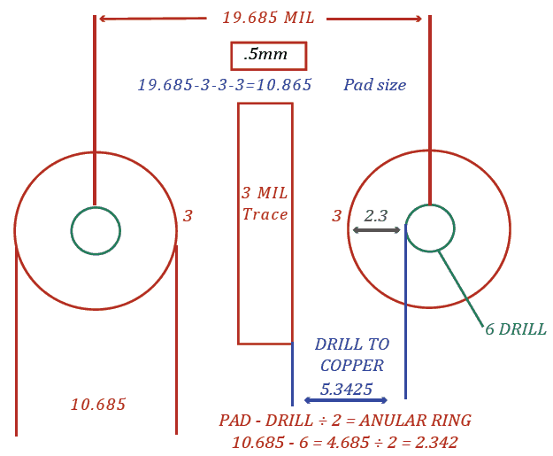
Now take the pad size of 10.685 mils minus the 6-mil drill size divided by two and you have a 2.3425-mil annular ring on the pads.
10.685 – 6 / 2 = 2.3425
Need help breaking out BGAs? Our engineering team can assist you with fanout strategies, via placement, and trace routing to ensure successful BGA escape routing.
You can book a meeting with our experts or call us at +1 (800) 763-7503.

On a plane layer:
If the via ties to the plane, it will be a solid tie (no thermal relief). If the via does not tie to the plane or to a signal trace on this layer, the pad on this layer can be removed. You can set up your design software to suppress unconnected pads, and it will remove the pads on non-functional pins.
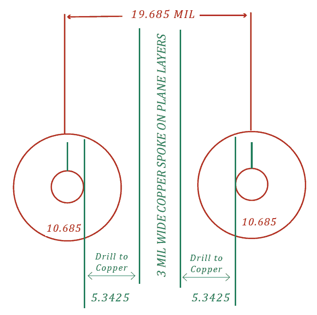
On a .5mm BGA, the copper spoke between the drills will be 3 mils wide. The distance from the edge of the drill to the edge of the 3-mil copper spoke between the drills is the drill-to-copper spacing. With the above sizes, the drill-to-copper will be 5.3425 mils. The drill-to-copper spacing required to manufacture the PCB changes due to many different factors. There is no set rule of thumb size for all boards.
This works if the board is 62 mils or less thick and does not have more than eight layers. The board thickness and the layer count have an increase in cumulative tolerances, which explains why fewer layers on a thinner board help a lot.
Set up the footprint of the part with the via-in-pad – ie, a drill in the surface mount component pad of the BGA.
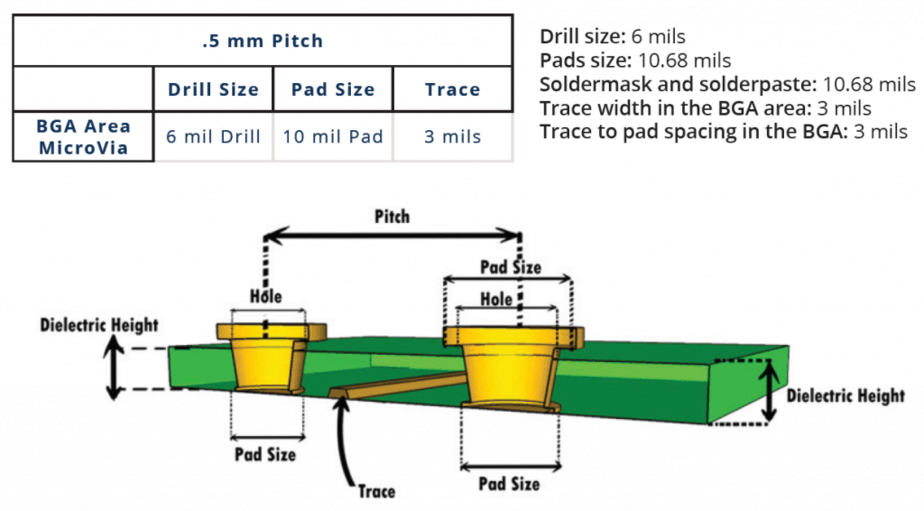
Drill size: 6 mils
Pads size: 10.68 mils
Solder mask and solder paste: 10.68 mils
Trace width in the BGA area: 3 mils
Trace to pad spacing in the BGA: 3 mils
The manufacturer might adjust the trace and space a little, but can build the board with these numbers.
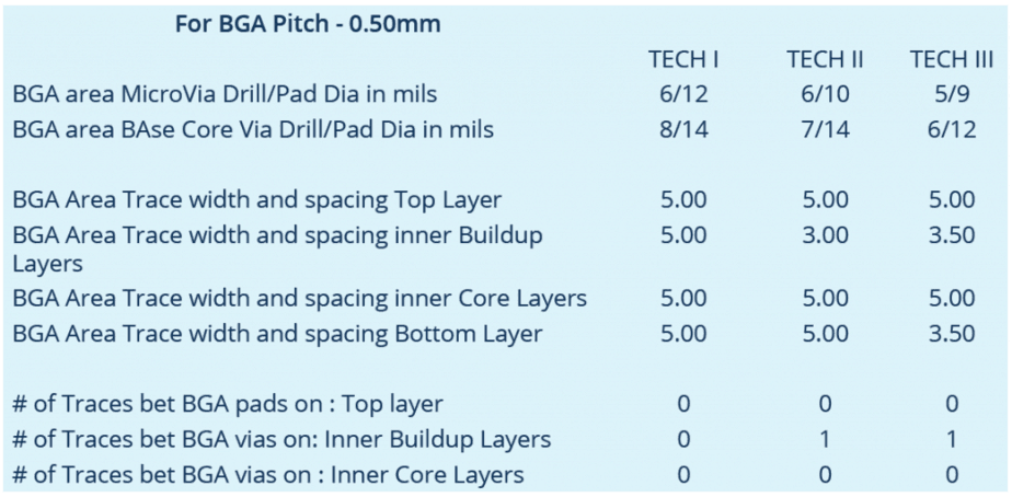
Breakout a .5mm pitch
Breakout a BGA: Technology level for .5mm

Is the high-density interconnect technology your strong suit? Take this HDI quiz and find out.
For more information on design rules, check with our DESIGN SERVICE team.


