Avoid component procurement delays by using a single vendor to source your parts. Transparent pricing. Fast turn-times.
Component Selection
When do I need to choose components?
It can come in handy to choose components early in the design process. This is the best way to ensure there are no conflicts between the actual design and the components being assembled. If you factor in component sizes from the very beginning, component space and sizes are no longer a concern and the PCB assembly process can proceed without barriers.
What type of components should I go for?
Component availability can potentially cause significant delays. You can avoid this issue by checking the availability of all components before beginning the design. If there are parts which require long lead-times, they can be ordered early and be consigned to the PCB assembly vendor. The assembly vendor can also handle the procurement of the more widely available parts, so every component will be ready and waiting when your boards are ready to be assembled.
Is reballing a necessary step in the leaded soldering process?
Reballing ensures higher reliability of your circuit. It effectively addresses issues like bad solder joints and mitigates problems associated with loose connections in the leaded soldering process.
Layout and Design
How important are component footprints?
Component footprints are another major aspect of layout design. A PCB master will make sure their footprints are created accurately as per the land pattern recommended in the datasheet. It is very important to use the numbering key correctly from the datasheet to identify the correct part and its land pattern. Reading the datasheet incorrectly will result in an incorrect footprint, which could require a complete redesign and re-fabrication of the boards.
Do I need to pay attention to part-to-part spacing?
One of the frequently asked questions posed by designers who are not yet PCB masters is in regard to the component-to-component spacing. Placing components too closely together can create various issues which may require redesign and refabrication, resulting in loss of time and money.
BOM
Should I keep my BOM up to date?
A BOM is a key aspect of both design and assembly. If there are any issues in your BOM, the assembly house will place the project on-hold until the issues have been resolved with an engineer. One way to make sure your BOM is updated is to review your BOM any time there is a change in your design. When you add new components to your schematic while the layout is in process, make sure you’ve also updated the BOM with the correct part number, description, and component values.
Use the BOM Checker to ensure your bill of materials is error-free.
If I send short tape ICs, will it cause any delays?
If it’s a short tape, we can extend the tape and make it a little longer. Let’s say you send in a 2-inch tape, we can make it to 6 inches. Although, it does take some time to do this. We recommend not to send in a 30-line item BOM all with short tapes because we would not process that.
Mixing Technologies
Can I mix technologies?
Our best advice would be not to. The payoff of a single through-hole, for example, doesn’t outweigh the additional time and money spent. It would be more efficient to either use multiple through-holes or none. If you do use through-hole technologies, placing all through-holes on one side of the board will reduce manufacturing time.
Package Size
How do I pick the appropriate package size?
It is important to choose the appropriate package size while in the PCB design phase. Ideally, you would only choose smaller packages when there is a good reason to; otherwise, lean toward bigger options. In too many cases, electrical engineers choose unnecessarily small component packages. This can create issues in terms of assembly yield, as it is more difficult to touch up and rework smaller components. Depending on the amount of rework needed, it may be more cost-effective to completely rebuild the board the remove and solder on new components.
Kitting & other component guidelines
What are the mandatory PCB assembly data required for kitting components?
The mandatory PCB assembly data required for kitting components are:
- Gerber/CAD/ODB++ files
- BOM of the desired PCBA in Excel (.xlsx) format
- X-Y data for the BOM
- Assembly drawing
- Special instructions for assembly, if any
What is the additional information required for kitting that can help in a faster deliver?
The following data if specified in advance, can speed-up the assembly process:
- Assembly required is RoHS or non-RoHS or leaded?
- Flux to be used – clean or no-clean?
- IPC standard required for assembly –
- IPC-A-610 – class II or class III or any other?
- After assembly PCB cleaning – required or not?
- Conformal coating – required or not?
- X-ray inspection- required or not?
- Ionic contamination report – required or not?
- Any testing requirements like functional testing/flying probe testing/electrical testing etc. needs to be specified
- Separate documents can be provided for special instructions for assembly/rework/modification if any.
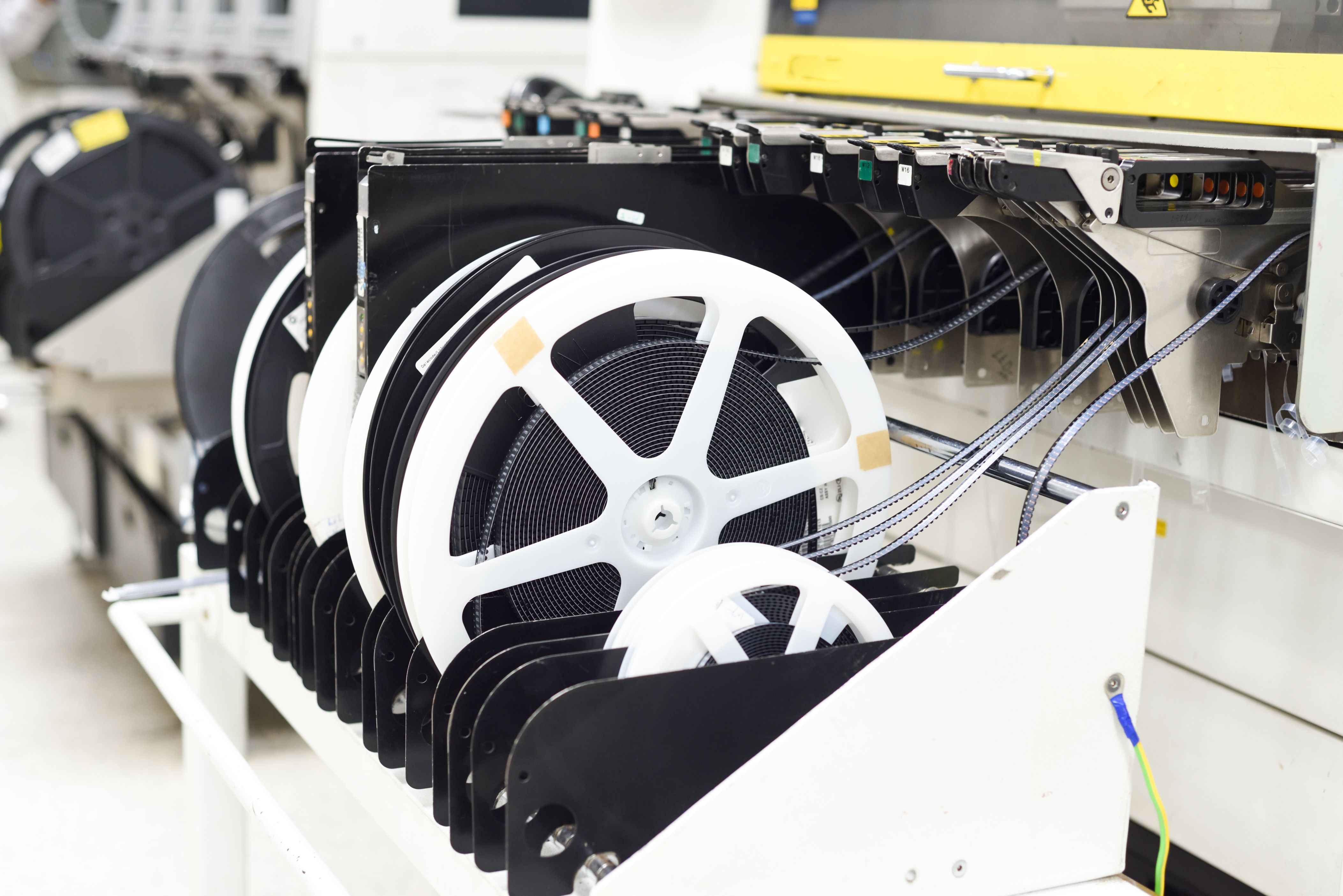
Does Sierra need reels or can you handle shortcut tape?
We need reels (packaging of components) to prevent damage during transport, handling, and storage purposes. In this packaging method, electronic components are fed into separate pockets which meet the design specifications. These pockets are molded into an air-tight, dust-free plastic tape that serves as a shield for them. The tape holds every part in place and organizes them into a connection string.
Along one edge, this tape has a row of pocket holes that allow for indexing. The tape is then machine rolled around a clean, strong plastic reel. Finally, it resembles a film tape and reel device.
Advantages
- Allows precise orientation of parts to customers’ assembly line equipment.
- Packaging can be adapted according to different component specifications.
- Protection from damage and electrostatic discharge during shipping.
- Reel provides rigid protection of tape and parts during shipping and handling.
Surface mount reels
The surface mount reels are made from high-impact and general-purpose polystyrene for added strength and durability. These reels are available in a variety of widths with anti-static coating.
Through-hole reels
Through-hole reels consist of corrugated reel flanges, spiral wound core, and hubs made of either plastic or metal. Depending upon the packaging requirements, different core lengths are used.
Where should I deliver all the kit components?
We require all parts to be delivered to Sierra Circuits, Inc. Attn: (mention work order# or quote# here), 1980 Lundy Ave (receiving department), San Jose, CA 95131. We should receive all the components by 1:00 PM PST. Any board received after this time will be processed the following day.
See our FAQs on customer consigned inventory for guidance on a successful consignment.
Capabilities
Can Sierra reball to leaded solder?
Yes, we can.


