Parasitics in PCB components introduce unwanted capacitance, inductance, and resistance, transforming ideal parts into complex RLC networks. This distorts impedance, shifts resonance points, and degrades signal integrity at high frequencies.
As a result, designs that pass schematic checks and simulations can still fail EMI testing or exhibit excessive power noise after assembly. This is due to parasitic effects that originate from parts and copper features on the circuit board.
To prevent these failures, layout and signal integrity engineers should choose components by considering self-resonant frequency (SRF) and model real-world behavior during simulation.
In this article, you’ll learn how parasitics impact electronic parts, alter high-frequency performance, and design strategies to manage undesired capacitance and inductance.
Highlights:
- Choose components based on frequency behavior, not nominal values.
- Consider parasitic effects during simulations to prevent late-stage EMI and power-integrity failures.
- Select decoupling capacitors based on SRF and operating frequency.
Why does component performance degrade in high-speed PCBs?
At high frequencies, parasitic capacitance and inductance dominate a component’s electrical response, altering how it interacts with signals and power rails. These unintended effects can negate the part’s intended function and degrade overall circuit performance.
From a layout perspective, no passive device behaves as an ideal single element. Instead, each electronic component exhibits additional parasitic effects introduced by its internal construction and package geometry.
This behavior is commonly modeled as an equivalent RLC network rather than an ideal capacitor, inductor, or resistor. A real-world capacitor functions as a series RLC network, exhibiting equivalent series inductance (ESL) and equivalent series resistance (ESR).
ESL is the unintended inductance introduced by the component’s leads, terminations, and internal current loop geometry.
ESR is the effective internal resistance of a component caused by conductor losses, dielectric losses, and contact resistance.

Key contributors to component failure include:
- Parasitic inductance (Lₚ): Present in component leads, terminations, pads, and internal structures.
- Parasitic capacitance (Cₚ): Forms between parallel leads, internal windings, or electrode layers.
- Parasitic resistance (Rₚ): Exists within conductive materials due to losses.
For example, a bypass capacitor operating in a high-speed circuit may behave as intended at low frequencies. However, beyond its self-resonant frequency, parasitics in PCB components can cause the capacitor to behave inductively, defeating its filtering purpose and increasing noise instead of suppressing it.
For layout strategies, download the High-Speed PCB Design Guide.

High-Speed PCB Design Guide
8 Chapters - 115 Pages - 150 Minute ReadWhat's Inside:
- Explanations of signal integrity issues
- Understanding transmission lines and controlled impedance
- Selection process of high-speed PCB materials
- High-speed layout guidelines
Download Now
How self-resonant frequency defines part behavior
To understand the effects of parasitics in a PCB component, you need to evaluate its SRF.
It is the frequency at which a component stops behaving as intended. For example, a capacitor begins to act like an inductor. This transition directly affects decoupling effectiveness, impedance control, and high-frequency noise suppression.
This transitional behavior of a capacitor occurs as it contains both capacitance and parasitic inductance, and their reactances change differently with frequency. Capacitive reactance (XC) decreases as frequency rises, following the relationship 1/(2πfC). Conversely, inductive reactance (XL) increases with frequency according to 2πfL.
As shown in the graph below, at lower frequencies, the capacitive element dominates. However, a specific frequency exists where capacitive and inductive reactances exactly cancel each other, producing a minimum-impedance condition known as SRF.

The table below summarizes how a capacitor behaves when operating at different frequencies.
| Operating frequency region | Component behavior | Impedance response | Design implication |
|---|---|---|---|
| Below SRF | Acts as a capacitor | Decreases with rising frequency | Ideal for decoupling |
| At SRF | Purely resistive | Minimum impedance | Most efficient filtering point |
| Above SRF | Acts as an inductor | Increases with frequency | Inefficient filtering |
Need reliable high-speed boards with signal integrity?
Talk to a PCB expert: Book a meeting or call us at +1 (800) 763-7503.
How to manage parasitic effects in circuit board components
Parasitics cannot be eliminated, but they can be controlled through layout, component selection, and accurate modeling. By optimizing decoupling networks, using realistic simulation data, and accounting for transition effects, you can keep impedance low and maintain signal integrity.
Stick to these guidelines to manage parasitic effects in components:
1. Employ an effective decoupling strategy for high-frequency noise
Effective power distribution network (PDN) design relies on a tiered filtering approach that accounts for frequency-dependent parasitics. A single high-value capacitor cannot provide broadband noise suppression, as its equivalent series inductance limits high-frequency performance.
To avoid this:
- Select smaller package sizes (0201 or 0402) to minimize current loop area and reduce ESL.
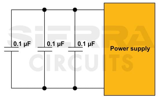
- Deploy parallel capacitor arrays with the same values to maintain low impedance across a wider frequency range.

Multiple decoupling capacitors in parallel with a power supply to maintain low impedance. - Place high-frequency decoupling capacitors close to IC power pins to minimize mounting inductance introduced by routing.


2. Account for via transition effects
Each layer transition introduces a parasitic discontinuity that alters transmission-line impedance. Via pads contribute parasitic capacitance, while the plated barrel introduces inductance proportional to its length.

Follow these strategies to avoid via transition effects:
- Remove non-functional pads on internal layers to reduce capacitive loading.
- Reduce barrel length using blind or buried vias to limit inductive discontinuities.
- Adjust antipad geometry on reference planes to better control via impedance for high-speed signals.
Sierra Circuits fabricates PCBs with ±5% impedance tolerance. We add test coupons to each panel and validate the impedance to ensure it matches your requirements.
See our controlled impedance capabilities to learn more.
3. Leverage accurate simulation models
Conventional SPICE models often fail to capture parasitic poles and frequency-dependent losses present in multi-gigabit systems.
An accurate simulation must reflect the real electrical behavior of components and interconnects. This helps pass the EMI tests on the first attempt.
For better results:
- Use part manufacturer-provided S-parameter models to represent frequency-dependent impedance characteristics.
- Include dielectric loss tangent and conductor skin effect in transmission line models.
- Verify the PDN impedance profile to ensure anti-resonant peaks do not coincide with the device’s operating spectrum.
Parasitics in PCB components are unavoidable, but their impact on high-frequency performance is predictable and manageable. Selecting components based on frequency behavior, optimizing placement and routing, and using accurate simulation models help you avoid parasitic-related issues.


