Contents
S-parameters allow you to analyze circuit behavior by characterizing how signals are transmitted and reflected through any device. A vector network analyzer (VNA) is used to measure these parameters accurately.
Highlights:
- S-parameters describe energy propagation in electrical networks and analyze voltage and currents at input and output ports.
- They help you understand the root causes of BER, ground bounce, EMI, and jitter in PCBs.
- VNA uses frequency-domain analysis for accurate S-parameter measurements.
- They support high-speed design by identifying loss, reflections, impedance issues, and crosstalk.
In this article, you will learn how S-parameters help in signal integrity analysis, the instruments we use for measurement, and different S-parameters for multiport networks.
What are S-parameters?
S-parameters or scattering parameters describe how RF or high-speed electrical signals behave when they encounter a circuit, component, or network. It explains how energy can propagate through an electrical network. Scattering parameters depict a complex network as a black box, analyzing the voltage and currents only at the input and output ports.
These are particularly used to describe a network in amplitude and phase vs. frequency. S-parameters offer comprehensive insight into the linear behavior of RF and microwave components.
As well as they also describe how the component under test interacts with other devices when they are cascaded. The parameters are an integral part of the theories for filter, transmission line, and amplifier design.
S-parameters provide the quantitative analysis for comprehension of the root causes of bit error rate (BER), ground bounce, EMI, and jitters in PCBs. You can measure crosstalk using scattering parameters to characterize signal transfer among adjacent transmission line pairs.
Various electrical standards like 10GbE (10-Gbps Ethernet), peripheral component interconnect express (PCIe), serial advanced technology attachment (SATA), and fiber channels all use S-parameters in their compliance test procedures.
Typically, S-parameters are saved in Touchstone format with a .snp extension, where n is the number of ports. Many electronic design automation (EDA) and circuit simulation software tools allow you to view and plot 2-port and 4-port S-parameters from Touchstone files.

Signal Integrity eBook
6 Chapters - 53 Pages - 60 Minute ReadWhat's Inside:
- Impedance discontinuities
- Crosstalk
- Reflections, ringing, overshoot and undershoot
- Via stubs
Download Now
How are S-parameters measured?
S-parameters are measured using a vector network analyzer. It’s a specialized instrument that sends known signals into an RF/microwave device and captures how much of that energy is reflected and transmitted at each port.
Each S-parameter (Sij) has a real magnitude and a phase in the complex part.
These are defined as the ratio of the sine wave voltage leaving a port to the sine wave voltage entering the port.
Sout-in = Sij = Vout / Vin
Let’s see how S-parameters apply to different network configurations.
1-port network
A 1-port DUT has one S-parameter (S11). It is the ratio of the output voltage of port 1 to the voltage going into port 1. It is also known as return loss (RL) as a measure of reflected energy out of port 1.
In electrical circuits, a port includes a pair of terminals connecting an electrical circuit or network to an external device or a circuit.
The external device will act as a point of entry or exit for electrical energy. Ports must satisfy the condition that currents flowing into the two nodes must be equal and in opposite directions.

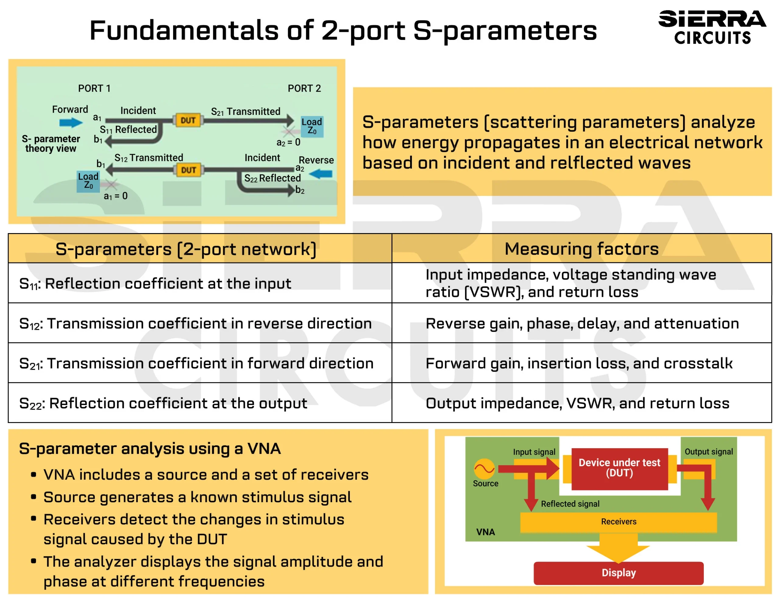
2-port network
Two-port network theory is a circuit analysis technique to describe a circuit concerning two terminals by considering a circuit as a two-port network.
In most electrical networks, obtaining the voltages and currents at the input and output ports is more convenient and practical than at any defined point in the circuit.
The basic methodology here is that only the terminal variables, such as input current/voltage and output current/voltage, are considered for analysis. The voltages and currents within or inside the circuit are not considered here.

In other network analysis techniques, such as Kirchhoff’s laws or superposition theorem, one can calculate voltages and currents at any point in the circuit. Thevenin’s equivalent and Norton’s theorems enable one to obtain an equivalent circuit at specified terminals in the network.
Here’s a quick infographic on 2-port s-parameter basics:
4-port network
A 4-port DUT has 16 S-parameters divided into four quadrants, as shown in the image. Here, the number of possible S-parameter combinations is the square of the number of ports.
In this example, the top left quadrant 1 and bottom right quadrant 4 are the same as individual 2-port DUTs with different port indices.
| Quadrant | Sxx (col 1) | Sxx (col 2) | Sxx (col 3) | Sxx (col 4) |
|---|---|---|---|---|
| First quadrant | S11 Ratio of the voltage coming out of port 1 to the voltage going into port 1. Reflection loss out of port 1 |
S12 Ratio of the voltage coming out of port 1 to the voltage going into port 2. Insertion loss from port 2 to port 1 |
S21 Ratio of the voltage coming out of port 2 to the voltage going into port 1. Insertion loss from port 1 to port 2. For uniform transmission lines, S21 = S12 |
S22 Ratio of the voltage coming out of port 2 to the voltage going into port 2. Reflection loss out of port 2. For uniform transmission lines, S11 = S22 |
| Second quadrant | S13 Ratio of the voltage coming out of port 1 to the voltage going into port 3. NEXT, coupling from port 3 to port 1 |
S14 Ratio of the voltage coming out of port 1 to the voltage going into port 4. FEXT coupling from port 4 to port 1 |
S23 Ratio of the voltage coming out of port 2 to the voltage going into port 3. FEXT coupling from port 3 to port 2 |
S24 Ratio of the voltage coming out of port 2 to the voltage going into port 4. NEXT coupling from port 4 to port 2 |
| Third quadrant | S31 Ratio of the voltage coming out of port 3 to the voltage going into port 1. NEXT coupling from port 1 to port 3 |
S32 Ratio of the voltage coming out of port 3 to the voltage going into port 2. FEXT coupling from port 2 to port 3 |
S41 Ratio of the voltage coming out of port 4 to the voltage going into port 1. FEXT coupling from port 1 to port 4 |
S42 Ratio of the voltage coming out of port 4 to the voltage going into port 2. NEXT coupling from port 2 to port 4 |
| Fourth quadrant | S33 Ratio of the voltage coming out of port 3 to the voltage going into port 3. Reflection loss out of port 3 |
S34 Ratio of the voltage coming out of port 3 to the voltage going into port 4. Insertion loss from port 4 to port 3 |
S43 Ratio of the voltage coming out of port 4 to the voltage going into port 3. Insertion loss from port 3 to port 4. For uniform transmission lines, S34 = S43 |
S44 Ratio of the voltage coming out of port 4 to the voltage going into port 4. Reflection loss out of port 4. For uniform transmission lines, S33 = S44 |
S-parameters in the top right quadrant 2 and bottom left quadrant 3 describe the near-end and far-end coupling of the ports. An unwanted coupling at the near-end of the transmitting port is called near-end crosstalk (NEXT), whereas the far-end coupling is known as far-end crosstalk (FEXT).

Advantages of using S-parameters
- S-parameters provide valuable insights into the performance of linear electrical networks, such as amplifiers, filters, and various RF components.
- They capture details on signal reflection, attenuation, signal magnitude, and phase.
- Extract various transmission line parameters using specific mathematical models and equations such as R, L, C, G, TD, and Z0.
- Optimize the circuit performance by pinpointing the locations of signal loss and impedance mismatches.
- S-parameters of an S-matrix can be easily transformed into other parameters, including Z-parameters, Y-parameters, H-parameters, T-parameters, and ABCD-parameters, providing flexibility and convenience in analyzing and designing electronic circuits.

Fill out the form:
What are S11 and S21?
S11 and S21 are input reflection and forward transmission coefficients, respectively, in a two-port network.
What is the reflection coefficient (S11)?
The reflection coefficient is a quantity that describes how much of a wave is reflected by an impedance discontinuity in the channel of transmission. It can be defined as the ratio of the amplitude of the reflected wave to the incident wave.

The graph above shows a generic interpretation of a frequency response curve generated by vector network analyzers.
What is transmission coefficient (S21)?
The transmission coefficient (S21) tells us how the transmission line transmits the signal. It is related to the insertion loss in the transmission.

The theoretical depiction of S-parameters using a VNA S11 and S21 is calculated as follows:
a1 = traveling wave incident on port 1
a2 = traveling wave incident on port 2
b1 = traveling wave reflected from port 1
b2 = traveling wave reflected from port 2
A 2-port DUT has four S-parameters:
S11 = b1/a1 = the input reflection coefficient
S12 = b1/a2 = the reverse transmission coefficient
S21 = b2/a1 = the forward transmission coefficient
S22 = b2/a2 = the reverse reflection coefficient
What are reflections on transmission lines?
A signal that travels along an electrical path will tend to be partially or completely reflected in the opposite direction when it experiences a discontinuity in the line’s characteristic impedance.
Reflections also result when the far end of the transmission line is not terminated in its characteristic impedance. They can also occur when two line lengths of different transmission lines are joined together.
The reflections are measured as the ratio of the reflected signal to the incident one. Network analyzers enable you to conduct reflection measurements, measuring the incident and reflected signals.
PCB Transmission Line eBook
5 Chapters - 20 Pages - 25 Minute ReadWhat's Inside:
- What is a PCB transmission line
- Signal speed and propagation delay
- Critical length, controlled impedance and rise/fall time
- Analyzing a PCB transmission line
Download Now
Return loss
It is the signal loss caused by reflection or discontinuity in a transmission line. This parameter is expressed in decibels (dB), and it is a scalar (amplitude only) quantity.
A really well-matched DUT will cause a massive loss in the power reflected from the open. This leads to a higher return loss. With increasing reflections, a badly matched DUT will have a much lower loss, making its return loss really small.

Insertion Loss = incident power/ transmitted power
Return Loss = incident power/ reflected power
In logarithmic terms, the formula for return loss is given as:
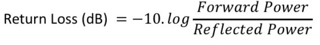
Even if the measured reflection value on the VNA is -25dB, the negative sign is ignored when representing return loss; the component is said to have a loss of 25 dB.
Voltage standing wave ratio (VSWR)
Two waves traveling in opposite directions on the same transmission line cause a standing wave if they have the same amplitude and frequency. This occurrence can be measured using the voltage standing wave ratio (VSWR).
VSWR is defined as the ratio of the maximum reflected voltage to the minimum reflected voltage at a specified frequency. It is a scalar quantity that provides only the amplitude. This parameter varies between one for a perfect match and infinity for an open or short circuit or lossless reactance.

What is the difference between small-signal and large-signal S-parameters?
The main difference between small-signal and large-signal S-parameters is that the former deals with linear effects on a network or circuit. In contrast, the latter deals with nonlinear effects on a network or circuit. We will now discuss in detail what these two parameters mean.
Small-signal S-parameters
Small signals in this scenario refer to signals that only have linear effects on the network. The signal will qualify as a small signal when gain compression or other nonlinear effects do not occur.
Gain compression is said to take place when an amplifier’s input power is increased to a level that decreases the amplifier gain, causing a non-linear increase in output power.
Small-signal S-parameters are defined as the ratio of reflected and incident waves.
Regarding passive networks, small signals are the only concern regarding signal behavior, as they act linearly at all power levels.
Large-signal S-parameters
Large signals deal with non-linear circuits, and large-signal S-parameters are based on a harmonic balance simulation of the full non-linear circuit. Harmonic balance is a frequency-domain analysis method used for the simulation of distortion in nonlinear circuits and systems.
Large-signal circuit simulation methods include non-linear effects such as gain compression. This leads to a change in scattering parameters when power levels are varied.
It is also why large-signal S-parameters are called power-dependent S-parameters. Similar to small-signal S-parameters, large-signal scattering parameters are described as the ratio of reflected and incident waves.
The difference is summarized in the table below:
| Aspect | Small-Signal S-Parameters | Large-Signal S-Parameters |
|---|---|---|
| Signal type | Low-power, linear signals | High-power signals that introduce nonlinearity |
| Behavior | Network responds linearly; no gain compression or distortion. | Non-linear behavior occurs, includes gain compression and distortion |
| Definition | Ratio of incident to reflected waves under linear conditions | Ratio of incident to reflected waves under nonlinear, power-dependent conditions |
| Circuit type | Passive or linear circuits | Non-linear circuits and active devices under large drive levels |
| Simulation method | Linear small-signal analysis | Harmonic-balance simulation for nonlinear behavior |
| Power level influence | Independent of input power | Scattering parameters change with power level |
| Use case | Predicting the behavior of components in linear operating regions | Evaluating power-dependent performance, such as in amplifiers |
| Key focus | Stability, matching, and linear gain | Compression, distortion, and overall nonlinear response |
Mixed-mode S-parameters
Signal integrity engineers often must check transmission line models and S-parameter measurements against frequency vs. gain compression plots (Cartesian coordinates) or Smith charts (polar coordinates). Most such plots are expressed in mixed-mode S-parameters for differential transmission lines.
Mixed-mode scattering parameters are a set of network parameters used to characterize the near-end (NEXT) and far-end crosstalk (FEXT) in differential circuits. The matrix comprises four outcomes in response to an input signal.
| Type of quadrant | Input excitation | Output response |
|---|---|---|
| First | Differential | Differential |
| Second | Common | Differential |
| Third | Differential | Common |
| Fourth | Common | Common |

3 key instruments to measure signal integrity
Oscilloscopes, TDRs, and VNAs are the primary instruments used to measure signal integrity in high-speed digital systems. As data rates push into the multi-gigabit range, channels face tighter timing margins, increased intersymbol interference (ISI), and higher crosstalk, making accurate characterization of reflections, losses, and coupling essential.
In the constantly evolving computing field, the shift from parallel to high-speed serial data transmission gives rise to new PCB design challenges.
Data rates are increasing, pushing more bits per unit of time through a single interconnect link/channel. These data rates have been nearing the Gigabit-per-second regime, leading to tighter timing budgets.
Intersymbol interference is a type of signal distortion in which one symbol interferes with consecutive symbols. This is an undesired event as the previous symbols have a similar effect as noise, affecting the reliability of the communication.
Due to high-frequency interconnect losses, a higher data rate will lead to higher ISI. Another important consideration is higher data transmission rates requiring multiple serial links to work in parallel, generating multilane configurations. This will lead to crosstalk issues.
This is why you must manage the characterization of channel reflections, losses, and crosstalk. Such characterization must be done in the frequency domain rather than the time domain using S or scattering parameters.
Two fundamental measurement methods are available for signal integrity characterization of channels in digital systems: time domain reflectometry (TDR) and vector network analyzer.
1. Oscilloscope
Oscilloscopes are multi-functional devices that offer a graphical representation of electrical signals. They enable direct observation of phenomena like ringing, intersymbol interference, noise, jitter, and differential skew.
The steps involved in oscilloscope operation are as follows:
- Connect a probe to the circuit under test to capture the input signal. The oscilloscope then amplifies the desired signal to a level suitable for display.
- Control the horizontal and vertical deflection of the waveform to represent time and voltage scales, respectively.
- Adjust time base and trigger settings to control the time axis and trigger conditions for signal display.
- The processed waveform is displayed on a screen, which can be a cathode ray tube (CRT) in analog oscilloscopes or an LCD/LED screen in digital oscilloscopes.
2. Time-domain reflectometer
The time-domain reflectometer is an electronic device that uses reflected waveforms to decipher the characteristic impedance of PCB traces, a cable, a connector, or any other transmission line. It checks for electrical discontinuities.
In the early days of signal integrity measurement, the TDR displayed the reflection coefficient or impedance versus distance.
The location and nature of the electrical discontinuity can be precisely determined based on the timing, phase, and amplitude of the reflected waveform. TDR translates the reflected waveforms to generate a graphical representation of discontinuities in a transmission channel.
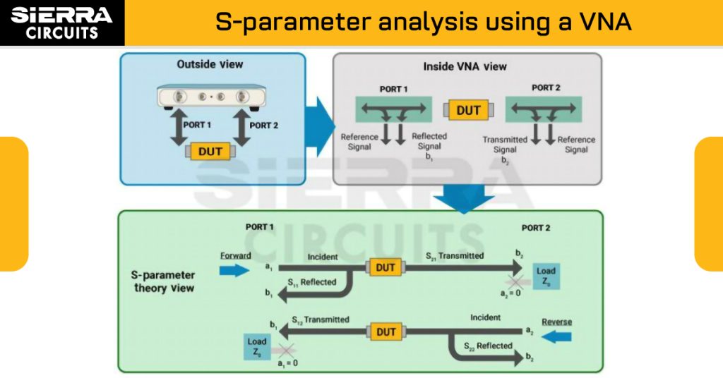
3. Vector network analyzer
A VNA includes a source that is used to create a known stimulus signal and a single receiver or a group of receivers that are used to detect changes to the stimulus signal caused by the device-under-test, or DUT.
A DUT is a manufactured product subjected to testing, either right after manufacturing or later during its life cycle, as part of ongoing functional testing and calibration checks.
The receivers of the vector network analyzer evaluate the resulting signals and compare them to the predetermined stimulus signal. It measures a component’s frequency response or a network of several components, which can be both passive and active.
A VNA measures the power of a high-speed signal that goes into and comes out of the component or network. This is because power, when compared to voltage and current, can be measured accurately at high frequencies. VNAs capture both the amplitude and phase of the signal at every point.
By evaluating the phase and magnitude of the signals, a wide range of device characteristics, such as impedance, return loss, insertion loss, and group delay of the signals, can be measured.
Most VNAs today are multipath instruments with multiple ports, where stimulus signals can be applied to any port. The transmitted and reflected signals can be measured with a 2-port 1-path VNA to arrive at S11 and S21 values, but the DUT needs to be reversed to obtain the opposite parameters, S22 and S12.
A 2-port, 2-path VNA can reverse the signal flow. Here, the device can be connected to either port in either direction to measure the reflections at both ports and the forward and reverse transmission coefficients (S21 and S12).
The reference plane in a VNA measurement is the area of the device where the user calibration is carried out, and measurements are taken. The position of the reference plane influences the assessments. Apart from that, several instrumental errors can be corrected by calibration.
Factors that contribute to the measurement error include:
- Port matching: Ideally, a 50 Ω VNA test port would measure exactly 50 Ω. In the real world, the port impedance might differ depending on how well the hardware was designed. It is seen that even for a VNA with well-designed hardware, the return loss is 20 dB. Hence, matching the source impedance with the load is crucial.
- Directivity: To measure the incident and reflected waves independently at the DUT’s input and output, a VNA uses separation hardware such as directional couplers. A perfect coupler should only detect the wave for which it is designed. But sometimes, a piece of the reflected wave that is going in the opposite direction of the source signal will be linked with the adjacent arm of the coupler, as seen in the image.

- Frequency response: A VNA includes many receivers, each having slightly varying frequency responses and coupling factors because of their unique signal paths. This results in inaccurate phase and amplitude measurement for frequency. The phenomenon is referred to as reflection and transmission tracking.
- Isolation: Although ports should have infinite isolation between each other, practically, a small portion of the signal detected at one port may leak into the receiver channels of another port. This is termed crosstalk, which can also be adjusted during the calibration process.
4 reasons to use VNAs
- Accurate system error correction: A vector network analyzer can conduct comprehensive system error correction of the testing tool accurately.
- Precise measurement of magnitude and phase: VNAs can precisely measure both the magnitude and phase attributes of the DUT.
- Vector reflection coefficient data: VNAs offer the necessary vector reflection coefficient data to create visual representations on a Smith chart.
- De-embedding and embedding techniques: Computational techniques, such as de-embedding and embedding techniques, eliminate the mathematical insertion of test fixtures.
S-parameters enable you to analyze complex networks’ behavior with ease, helping you accurately predict signals’ responses. Knowing the signals’ behavior is crucial to designing efficient controlled impedance PCBs.
Need assistance in analyzing the signal integrity of your design? Post your queries on our forum, SierraConnect, and our experts will answer them.

About Poulomi Ghosh : Poulomi is a microwave engineer specializing in EMI, EMC, RF, and high-speed electronics. As a senior technical writer at Sierra Circuits, she creates advanced engineering articles and webinars for hardware engineers and PCB designers.