


Contents

On-demand webinar
How Good is My Shield? An Introduction to Transfer Impedance and Shielding Effectiveness
by Karen Burnham
An efficient PDN design in PCBs ensures a stable power supply and consistent voltage levels across all components. To achieve this, you need to overcome several challenges, such as Joule’s heating effects and undesired voltage drops.
Malfunctions in your power distribution network might lead to impedance mismatches, power losses, overheating, and short circuits.
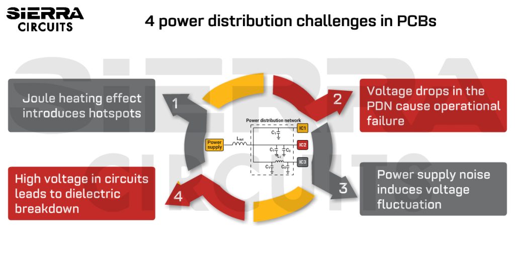
In this article, you’ll learn 4 common challenges in designing a power distribution network and ways to mitigate them.
Highlights:
For an efficient PDN design:
- Choose materials with Tg >160°C (EM-528, EM-827, and Ventec VT-447 FR4).
- Place a large decoupling capacitor (10 µF —100 µF) within 2 inches of the chip.
- Opt for larger via dimensions (0.031-inch hole and a 0.050-inch pad).
- Employ HASL (tin:~62% – Lead:~38%) surface finish.
4 PDN design challenges in PCBs
1. Joule heating effect introduces hotspots
The Joule heating effect occurs due to the resistance encountered by the current as it flows through the material. The resistance causes collisions between charge carriers and the material molecules, converting the electrical energy into heat. This phenomenon in power traces causes direct current losses and drops the voltage.
Impact of Joule heating on PCB power distribution:
- Temperature rise: Joule heating increases the temperature of conductive traces. This creates localized hotspots with uneven thermal distribution. Excessive temperature can affect the performance of electronic components, potentially causing them to fail.
- Increased resistance: The rise in temperature can also increase the trace resistance. This, in turn, affects the power distribution as the voltage drop across the traces may increase.
11 design tips to address heat dissipation challenges in PDN
- Select PCB materials with lower thermal resistance. These materials offer better thermal conductivity, helping dissipate heat more effectively. For instance, Fujipoly’s new Sarcon® 30-YR is a thin film exhibiting a thermal conductivity of 2.2 W/m°K with a thermal resistance of 0.28°Cin2/W at 0.3mm thickness.
The type of materials you choose defines the quality of your end product. Download our PCB Material Selection Design Guide to learn how to select the right substrates for your design.

PCB Material Design Guide
9 Chapters - 30 Pages - 40 Minute ReadWhat's Inside:
- Basic properties of the dielectric material to be considered
- Signal loss in PCB substrates
- Copper foil selection
- Key considerations for choosing PCB materials
Download Now
- Use thicker copper layers (1 oz-2 oz) to increase the Cu area for high-current paths and improve the trace conductivity.
- Minimize the length of power distribution traces to reduce resistance. Keep the distance between the power source and loads as short as possible.
- Implement copper pours in your layout to distribute heat effectively. They act as heat sinks.
- Use thermal relief pads for vias connected to power planes; these pads have reduced copper coverage, making it easier for heat to dissipate.
- Integrate heat sinks on components that generate more heat (ICs and BGAs) to increase the component surface area for effective heat transfer. Place thermal vias around the power component. These vias conduct heat away from the PCB and help in efficient thermal management.

Thermal vias for heat dissipation in PCBs Here’s what Keven Coates, a senior electrical engineer in avionics, has to say about PCB heat dissipation techniques.
- Add temperature sensors to critical components such as the CPU and motherboard. They provide feedback to the system to adjust power distribution if necessary.
- Increase the power trace width by around 10 mil (for 2 oz Cu thickness) to minimize resistance and voltage drop. Lower resistance leads to less heating for a given current. Balance the trade-off between wider traces and additional board area.
![]()

- Have current-limiting mechanisms such as fuses, circuit breakers, and pyrolytic films to prevent excessive heating. Additionally, use thermally conductive adhesives (TECA) to reduce the risk of localized heating in critical components.

Heat sink mounted on a high-power component. - Employ HASL (Tin:~62% – Lead:~38%) surface finish to minimize trace resistance. HASL inhibits CAF growth, which causes arcing. Choose ENIG for a thinner finish.
- Use simulation tools to analyze the thermal effects and changes in the electrical performance of the circuit board design. Joule heating simulation helps you understand how trace/via geometry, component density, and line resistance collectively influence the system.
For more on thermal management techniques, see 12 PCB thermal management techniques to reduce PCB heating.
2. Voltage drops in the power distribution network cause operational failure
When supplying current to a load, there might be a sudden voltage drop due to resistance (IR-based voltage drop). You must consider this loss during the layout phase and placement of the DC supply rails. The DC line voltage should not exceed the operating range of the connected components.

Voltage drops can lead to inadequate voltage levels at the end of power lines, affecting the reliability of the power supply. For ICs with low supply voltage requirements, even a small voltage drop can be significant.
In high-current circuit boards, the voltage drop becomes particularly noticeable and generates excessive heat. This heat can accelerate wear and tear on the cable insulation and may lead to premature failure of the equipment.

11 ways to deal with voltage drops in your PDN designs
- Opt for larger via dimensions, such as a 0.031-inch hole and a 0.050-inch pad, to enhance their current carrying capacity. Avoid using smaller vias, like a 6-mil via and 10-mil pad, for power delivery due to their limited current capacity. Larger vias, in combination with additional copper plating, prevent overheating and minimize voltage drops. However, they consume more board space and may complicate the layout process.
- Place vias strategically to minimize the loop area of the power and ground traces. A shorter path helps reduce inductance and voltage drops.
- Ensure a continuous plane without splits to reduce the loop inductance of the power distribution system.
- Place high-current components closer to the power source to minimize the loop length.
- Ensure the total current drawn by various circuit blocks does not surpass the rated output capacity of the power regulator.

Current drawn by a circuit block in PCB - Place bypass capacitors (tantalum or ceramic) near sensitive components to address sudden voltage spikes. They act as charge reservoirs and can release this stored energy quickly during high current demands and switching events. This rapid response helps maintain a stable voltage across the circuit and mitigate ground bounce.

Bypass capacitor model - Employ a high-voltage DC rail, such as a 48V or a dual 12/12V setup, as the primary power source. Introduce an intermediate bus converter that typically steps down the voltage to an intermediate level. Further, place multiple local point-of-load (PoL) DC-DC converters close to their respective loads. This addresses the IR drop (voltage drop due to current flowing through resistance) problem and greatly reduces noise pickup in the power rails.
- Use remote sensing, a variation of Kelvin sensing. It has two additional leads, so it can sense the voltage at the load and dynamically adjust its output to maintain that value despite the IR drop.
- Opt for 2-3 oz copper cladding for high-current circuits, power electronics, and applications with stringent thermal requirements. This effectively reduces the resistance by half. On the other hand, thicker cladding raises costs and PCB fabrication complexity, requiring a cost-benefit analysis before implementation.
- Employ a stand-up bus bar to route the power lines. Even if the board is a low-profile SMT design, there’s usually headroom for a low-profile bus bar that can be relatively thick, providing a low-resistance DC path. Many of these bars are offered as two-layer (or more layers) structures, with one layer for the supply rails and the other for the ground return.
- Utilize power distribution network simulators for the analysis and computation of voltage drops throughout the PDN. These simulators verify if the integrated circuits in your layout receive the desired voltage.
Need help in optimizing your PDN for minimal impedance? Check out our PCB design support.
3. Power supply noise induces voltage fluctuations
Power supply noise originates from the power distribution system. This conducted noise spans a frequency spectrum ranging from 10kHz to 150MHz.
Here are some of the key effects of power supply noise on the PDN:
- Voltage ripple: Power supply noise can introduce variations in the voltage level across the PDN. High-frequency noise can cause voltage ripple, the periodic variation in the DC voltage level. This can affect the stability of the power supply to components.
- Resonant and anti-resonant peaks: Power delivery networks that are not properly impedance-matched may exhibit resonant and anti-resonant peaks in their impedance spectrum. This can lead to large voltage spikes at specific frequencies, contributing to power supply noise.
- Power lines as EMI sources: Power distribution lines can act as unintentional antennas, radiating electromagnetic fields.
To learn how to minimize noise in high-power boards, see 7 PCB layout design tips for power electronics.
Using decoupling capacitors to reduce source noise
Decoupling capacitors are employed to filter out high-frequency noise that can induce voltage spikes in power distribution networks.

These capacitors act as local energy reservoirs, stabilizing power supplies and reducing noise-induced voltage variations.
- Place them as close as possible to the power and ground pins of the ICs to provide a low-impedance path for high-frequency noise.
- Use low-inductance surface-mount ceramic capacitors connected directly to the power supply pins of the ICs.
- Always connect the decoupling capacitors between the power source and the load/IC in parallel.

Various placements of decoupling capacitors in the PDN design - Opt for a higher number of capacitors to yield more favorable noise suppression. The optimal number depends on specific system requirements and constraints.
- Choose the capacitance value of the decoupling capacitors based on the PDN analysis. This analysis will help you determine the power delivery network’s impedance profile and the resonant frequencies to be avoided. Consider factors like:
- Target frequency range for noise suppression
- The target impedance value of different voltage rails of ICs
- Circuit board layout and trace lengths
- Current requirements of the ICs
- Desired roll-off characteristics
Desired roll-off characteristics define the rate at which the capacitor’s effectiveness in attenuating noise decreases with increasing frequency. They essentially describe the steepness of the transition from where the capacitor effectively shunts noise to where it loses its ability to do so.
- Place the lowest-value capacitor close to the IC’s pin, and consequently place higher-valued capacitors progressively farther away. Do not position the large electrolytic capacitor (typically 10 µF—100 µF) more than 2 inches away from the chip.

Arrangement of decoupling capacitors for noise filtering - When using vias to reach the power plane, establish a connection from the component pin to the capacitor first and then to the via to ensure a continuous current flow through the plane.

Component to power plane connection through a decoupling capacitor - Use via-in-pads to connect the power and ground planes with the shortest loop area.

Decoupling capacitor layout dos and don’ts - When selecting capacitors, consider frequency bands and resonance points to be suppressed. Lower equivalent series inductance (ESL) and equivalent series resistance (ESR) values are preferred for better performance. Ceramic capacitors can offer the lowest ESR and ESL values.

Alternatively, other technologies, such as tantalum capacitors, which offer high capacitance value in small packaging and low wear-out, can be suitable for specific applications such as military PCBs.
See power integrity in PDN design and high-speed simulations to learn about Steve Sandler’s insights on power integrity.
6 strategies to mitigate power supply noise
- Implement passive filters, such as inductors and capacitors, to suppress high-frequency noise.
- Maintain a minimum clearance of 50 mil between power traces and board edge.

Power trace to board edge spacing for an efficient PDN design - Introduce Faraday cage shielding in critical areas to contain electromagnetic fields and prevent radiated EMI from affecting nearby components or external systems.

Faraday cage at the board edge for noise isolation - Incorporate EMI shielding materials, such as conductive coatings (copper, silver, chromium, or nickel alloys) or metal shielding cans, in areas where electromagnetic radiation needs to be contained. This is especially important for sensitive components or areas prone to EMI.

Shielding protects the circuit from EM radiation - Employ transient voltage suppressors (TVS) such as TVS diodes, metal oxide varistors (MOV), or gas discharge tubes (GDT) to protect against voltage spikes and transients. TVS devices divert excess energy away from sensitive components, reducing the risk of EMI generation.
- Ensure compliance with relevant EMI standards and regulations such as FCC Section 15 and CISPR. Testing and certification processes can help verify that the PCB design meets industry requirements for electromagnetic compatibility (EMC).
For insights into designing highly complex PCBs with signal integrity, download the Signal Integrity ebook.

Signal Integrity eBook
6 Chapters - 53 Pages - 60 Minute ReadWhat's Inside:
- Impedance discontinuities
- Crosstalk
- Reflections, ringing, overshoot and undershoot
- Via stubs
Download Now
4. High voltage in circuits leads to dielectric breakdown
Dealing with high-voltage PCBs (above 30VAC or 60VDC) requires careful consideration of several design aspects to ensure the electronic system’s safety, reliability, and performance. Here are some common issues associated with high voltage in PCB power distribution:
- Dielectric breakdown: Excessive voltage can cause dielectric breakdown, where the insulating materials between conductive traces break down, leading to a short circuit.
- Trace overheating: High voltage can cause excessive current flow through traces, leading to resistive heating. Overheated traces can result in the degradation of the PCB material, increased resistance, and potential failure of the conductive paths.
- Voltage spikes and surges: Rapid changes in voltage, such as transients and surges, can occur for various reasons, including inductive loads turning on or off. These spikes can exceed the breakdown voltage of components, causing damage and reducing reliability.

Voltage spikes in PDN design. - Breakdown of isolation barriers: Circuit boards often have isolation barriers to prevent unintended current flow between different sections. High voltage can cause breakdowns in these isolation barriers. Unintended current paths can lead to short circuits, damaging components, and potentially causing catastrophic failures.
17 methods to improve power distribution in high-voltage boards
- Segregate high-voltage and low-voltage sections in your layout to prevent unwanted coupling. Use isolation barriers and dedicated areas for high-voltage components to minimize the risk of crosstalk and potential damage.
- Route high-voltage signals on the external layers for enhanced thermal dissipation. External layers have better thermal dissipation due to increased exposure to ambient air than internal layers.
- When routing high-voltage circuits, consider using cutouts to increase creepage. Avoid placing large holes, as they can cause issues with the board’s structural integrity, causing it to crack.

Grooves and notches increase creepage in your board layout - Adhere to appropriate clearance and creepage distances between conductors, especially in high-voltage areas. Follow industry standards and guidelines to determine the minimum distances required to prevent arcing and breakdown.
- Maintain sufficient clearance from board edges, mounting holes, and cutouts calculated based on the voltage requirements of the PCB, especially when routing on external layers. Refer to the IPC-2221 standards to get the required clearance. You can increase the spacing by 50 mil or more from the obtained value.
- Avoid sharp-angled traces and sharp-edged terminal pads in high-voltage connections to prevent charge accumulation. Instead, use elliptical pads and angular traces to avoid unintended consequences such as electrical breakdown and arcing.

Designing corner pads in high-voltage boards - Remove unnecessary copper pads in internal layers, especially in areas without connections. This optimization increases spacing in internal layers and contributes to better high-voltage performance.
- Choose materials such as EM-528, EM-827, and Ventec VT-447 FR4 with high Tg >160°C that can withstand high voltage levels. Materials with high breakdown voltages (>50kV) ensure the integrity of insulation between conductors.
- Utilize high-resin prepregs for inner layers with loose glass weave like 106, 1080, 2113, or 2116. Always consult your fab house when selecting materials to ensure they align best with your design specifications.
- De-rate the material’s electrical strength for long-term reliability. The de-rating value depends on factors like operating temperature, voltage stress duration, and material properties. You can get the de-rating factor in the material data sheet.
- Opt for insulation materials with higher CTI values (refer to IEC-60950-1 and IPC-2221 for some recommended materials). The comparative tracking index is a relative measure of an insulating material’s resistance to surface tracking. Higher CTI indicates better resistance to electrical breakdown. Furthermore, it also indicates a smaller distance requirement between PCB conductors, necessitating a minimum creepage value.
- Design high voltage traces with an adequate thickness of 2 to 3 Oz to handle the current without excessive resistance and heating.
- Implement guard rings around sensitive components like op-amp to divert stray current away from the sensitive node and minimize the risk of breakdown.
- Choose components that can safely handle high operating voltages, including capacitors, resistors, and semiconductors.
- Integrate overvoltage protection circuits such as transient voltage suppressors (TVS diodes) and varistors to safeguard sensitive components from voltage spikes.
- TVS diodes: Clamp voltage spikes above a certain threshold to protect sensitive components.
- Varistors: Offer nonlinear resistance that increases significantly with increasing voltage, limiting surge currents.
- Adhere to relevant safety standards and regulations, such as IPC-2221, IEC 60664, UL61010-1, and IEC-60601-1 (for medical electrical equipment). Additionally, adhere to the following measures to prevent high leakage currents in PCBs:
- Ground chassis/metal pipes to the earth
- Connect all earth connections of power systems to an earth bus bar/rods
- Use grounding wires to provide a low-impedance path for return currents
- Employ power surge and lightning protection devices, such as fuses and power isolators, to prevent damage
- Maintain detailed design documentation, including the specifications of high voltage components, trace widths, clearance distances, and any safety measures implemented. Clear documentation aids in troubleshooting and future modifications.
Why you should have a robust PDN design

1. Facilitates a stable power supply
Efficient power distribution ensures a stable power supply to all components on your board. This stability is essential for properly functioning integrated circuits and other components.
2. Minimizes undesired voltage drops
Voltage drops can occur when there is excessive resistance in the PDN. This can lead to lower voltage levels at critical points on the circuit board. Proper power distribution minimizes voltage drops.
3. Prevents ground bounce
The ground bounce occurs when the ground voltage fluctuates during signal transitions. It can lead to signal integrity issues and affect the performance of digital circuits. You can avoid this by designing an effective power distribution network.
4. Avoids localized overheating
Improper power distribution can lead to localized overheating, affecting the reliability and lifespan of components. Well-designed PDN helps distribute heat evenly across the board.
5. Reduces EMI
A robust power distribution system helps reduce EMI, which can impact the functionality of nearby electronic components. This is particularly important in sensitive applications where minimizing EMI is crucial.
Key takeaways:
- Increase trace width for power planes by around 10 mil for 2 oz Cu to minimize resistance and voltage drop.
- Minimize trace length and employ copper pour and thermal relief pads for better heat dissipation.
- Utilize stand-up busbars for low-resistance DC paths.
- Integrate overvoltage protection circuits, such as transient voltage suppressors (TVS diodes) or varistors, to safeguard sensitive components from voltage spikes.
- When designing PCBs to withstand high-voltage conditions, adhere to relevant safety standards and regulations, such as IPC-2221, IEC 60664, and UL61010-1.
An efficient PDN design is essential for a stable power supply. By employing the right strategies and adhering to best practices, you can overcome the challenges associated with PDN design.
TVS diodes and varistors suppress the ripple voltages while decoupling capacitors, and their proper placement can help filter out high-frequency noise and ensure a stable power supply.
Need assistance in designing a PDN for your circuit board layout? Post your queries on our PCB forum, SierraConnect. Our design and manufacturing experts will resolve them.

About Pooja Mitra : Pooja Mitra is an electronics and communication engineer. With an experience of over three years in the PCB industry, she creates industry-focused articles that help electrical and PCB layout engineers.


What simulation and testing methodologies do you employ to validate and optimize the performance of a PCB power distribution network?
How do you address challenges related to power integrity when designing PCBs with mixed-signal components, such as analog-to-digital converters or RF circuits?
Hey Madison! When dealing with mixed-signal PCBs, I’ve found that separating the analog and digital grounds really does the trick. It’s like giving each component its own space to play without interference. Also, don’t forget to connect those grounds at a single point – keeps things neat and tidy.
Totally agree. Decoupling capacitors have been my go-to. Placing them strategically near those mixed-signal components helps filter out the noise. Variety is the spice of life, right? So, use different capacitor values for a well-rounded noise filter.
Bypassing and filtering are key too. Low-pass filters are superheroes when it comes to taming high-frequency noise. And those ferrite beads in power lines? They’re like little noise ninjas. Trust me, your mixed-signal components will thank you.
Just wanted to jump in and mention isolation techniques. It’s like giving your analog components some “me time.” Physical barriers and isolation transformers can work wonders. Oh, and maintaining a solid power plane is non-negotiable for stable voltage. Don’t skimp on that!
I’d add controlled impedance to the mix. Keeping those power and ground traces in check minimizes reflections and maintains a smooth flow. Also, clock distribution is crucial – avoid skew and jitter like the plague.
Several tools are available to validate your board’s performance. Siemens EDA (formerly known as Mentor Graphics) provides a suite of tools, including HyperLynx for signal and power integrity analysis and Valor for ensuring compliance with manufacturing standards. Siemens Simcenter FloTherm can be utilized for thermal simulation.
Also, you can use Altium PDN Analyzer to optimize the circuit board’s power delivery efficiency and Cadence circuit simulation tools to verify the overall functionality and performance of the PCB design.
By leveraging these methodologies and tools, you can refine your design to ensure reliability.