PCB Stack-Up Design Guide
Sierra Circuits’ PCB Stack-up Design Guide provides practical guidelines for developing stack-ups that ensure manufacturability and signal integrity.


The guide covers stack-up construction methods and design considerations for different build-up types. It also provides practical guidance on fabrication documentation, DFM, and manufacturing tolerances to help you develop a layer stack that meets the fabrication requirements.
What you’ll learn:
- Why PCB stack-up planning is critical for reliable applications
- The functions of copper foil, prepreg, core materials, and key dielectric properties
- How stack-up construction affects signal integrity, controlled impedance, and power integrity
- Best practices for selecting layer count, arranging signal, power, and ground layers, and managing via transitions
- Different PCB stack-up configurations: multilayer, HDI, flex, rigid-flex, and hybrid boards
- How to document stack-up requirements in fabrication drawings and notes
- Common DFM issues, manufacturing tolerances, and build-up inspection methods
What is a PCB stack-up?
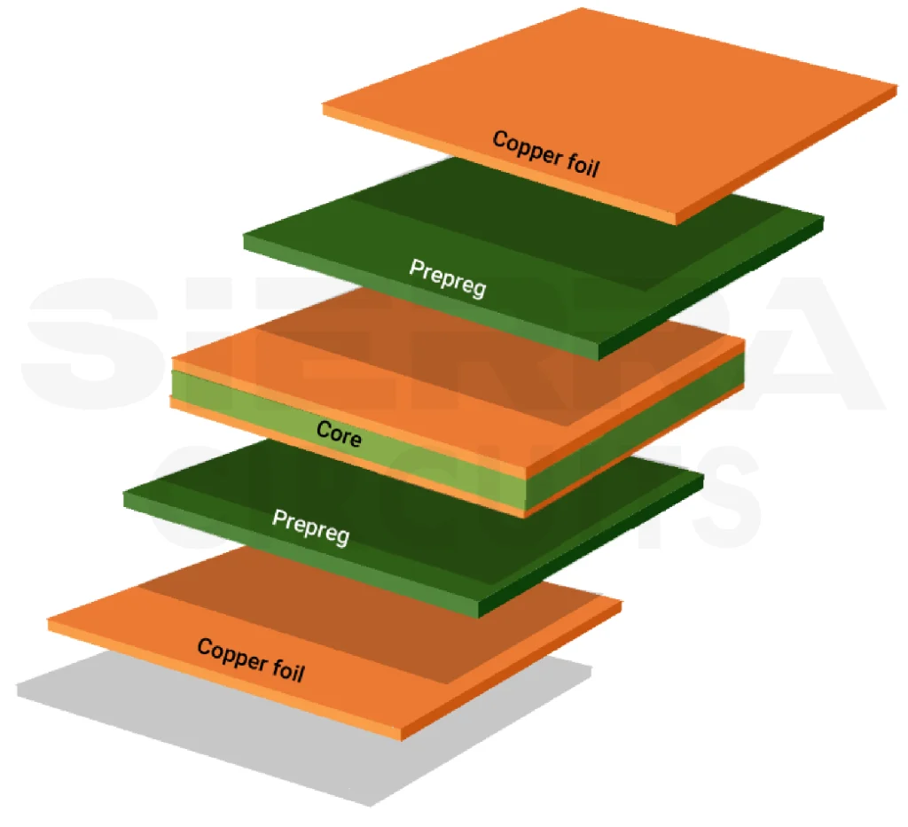
It is the sequence of conductive and dielectric layers that make up a circuit board. The layer stack establishes the board’s physical structure and provides the fabrication details needed to manufacture it accurately.
It specifies key construction parameters, including copper foil, laminates, board thickness, controlled impedance requirements, and the arrangement of signal, power, and ground layers. These aspects influence signal integrity, electromagnetic interference, mechanical stability, and manufacturing cost throughout the product lifecycle.
This design guide explains the essential elements of stack-up planning and their role in circuit board performance. It also outlines the information that should be defined before layout begins, helping you create layer structures that meet both electrical requirements and fabrication capabilities.
What materials are used in a PCB stack-up?
Copper foil, prepreg, and copper-clad laminates (cores) form the foundation of every circuit board stack-up. Copper foil creates the conductive paths for signals and power, prepreg electrically insulates and bonds adjacent layers during lamination, and the core provides structural support to the board. The guide explains how these materials are manufactured, the factors to consider when selecting them, and how each contributes to the finished stack-up.
The design guide also explains the dielectric properties that influence board performance, such as dielectric constant (Dk), dissipation factor (Df), coefficient of thermal expansion (CTE), glass transition temperature (Tg), decomposition temperature (Td), thermal conductivity, moisture absorption, flame resistance, and other mechanical characteristics. Understanding these properties helps you choose materials that align with your design’s electrical, thermal, and manufacturing requirements.
What are the different stack-up construction methods?
A multilayer board is either built using core construction or foil construction, depending on its electrical requirements, manufacturing constraints, and budget.
Each approach follows a different lamination process and offers distinct advantages for fabricating high-performance circuit boards.
Core construction uses pre-manufactured copper-clad core layers that are etched and bonded with prepreg to form the multilayer board. It is less flexible because core and copper thicknesses are available in standard sizes.
The guide explains how core construction works, where it is typically used, and the manufacturing considerations associated with this approach.
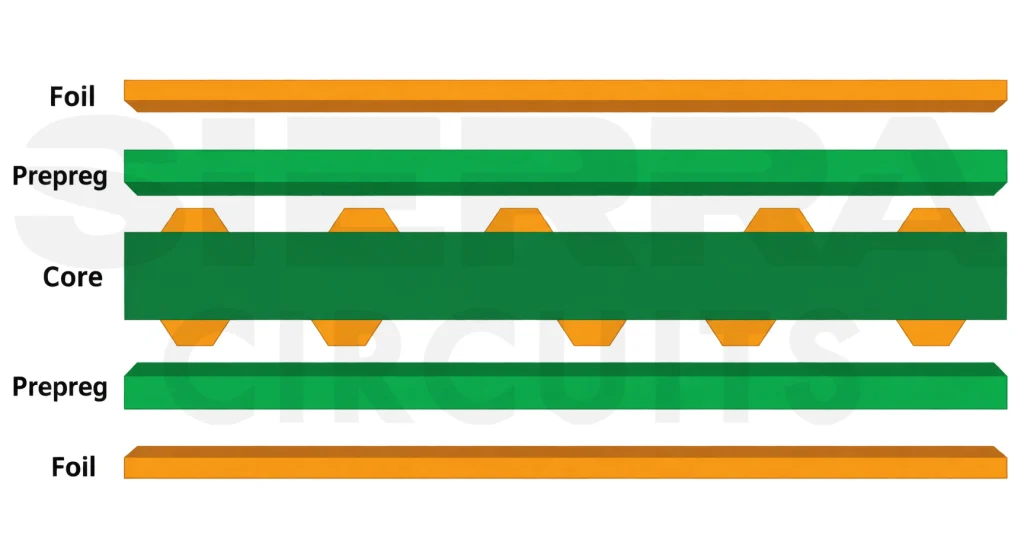
Foil construction uses individual copper foils, prepregs, and cores to build the layer structure through sequential lamination.
This method provides greater flexibility in selecting dielectric and copper thicknesses, supports blind and buried vias, and enables constructions tailored for controlled impedance and other electrical requirements.
The PCB stack-up design guide compares foil and core construction methods to help you choose the approach that best fits your design objectives and fabrication needs.
How does a stack-up affect a printed circuit board’s functionality?
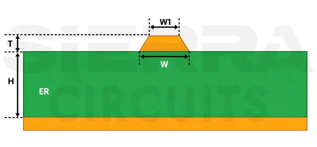
A well-planned PCB stack-up ensures efficient signal transmission, provides stable power, and guarantees a consistent impedance profile. Layer arrangement, dielectric materials, copper thickness, and reference plane placement determine how signals and power behave under different operating conditions.
These factors become increasingly important in high-speed designs, where poor layer planning can cause impedance mismatches, excessive noise, and unreliable circuit operation. Proper stack-up planning also helps minimize electromagnetic interference and supports consistent electrical performance.
This PCB stack-up design guide explains how to choose layer structures and materials for signal integrity, impedance control, and power distribution. It also covers practical considerations for optimizing board performance while supporting reliable fabrication.
How to design an efficient PCB stack-up?
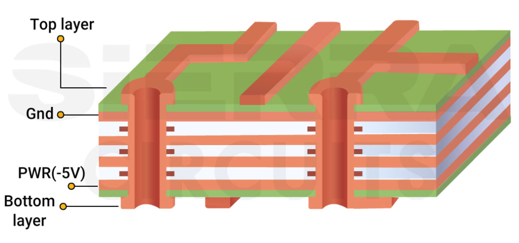
Start by selecting the layer arrangement, organizing signal and reference planes, and planning interconnections (vias). These decisions establish the foundation for routing, signal quality, power distribution, and overall board complexity.
The design process involves assigning functions to each copper layer, estimating the required layer count, placing signal, power, and ground planes, and determining how vias will connect them.
This guide explains how to plan the board structure, arrange conductive and dielectric layers, and implement layer transitions for different board designs. It also demonstrates how to use Sierra Circuits’ Stack-up Designer to create and evaluate stack-up configurations before finalizing the design.
What are the different types of circuit board build-ups?
Circuit board stack-ups can range from simple single-sided and double-sided designs to complex multilayer, HDI, flex, rigid-flex, and hybrid constructions
The layer count, materials, and fabrication methods vary across these designs, influencing their routing capability, mechanical flexibility, and manufacturing complexity. Single-sided and double-sided boards are commonly used for simpler products, while multilayer designs provide additional routing space for more complex circuits.
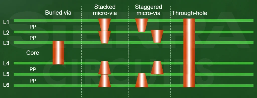
HDI boards incorporate sequential lamination and microvias to achieve higher interconnect density in compact electronics. Flex and rigid-flex constructions combine rigid and flexible sections to accommodate space-constrained or dynamic applications, whereas hybrid designs integrate different laminate materials to meet specific electrical and thermal demands.
The design guide explores each of these board types, explaining their construction, typical applications, and key design considerations. It also covers sequential lamination for HDI boards, materials used in flex circuits, and the design guidelines and manufacturing challenges associated with flex, rigid-flex, and hybrid constructions.
Together, these topics help you identify the most suitable board structure for your design objectives.
How to represent your stack-ups in fab drawings and notes?
Designers document the stack-up using layer detail tables, stack-up cross-sections, and fabrication notes that specify how to build the board.
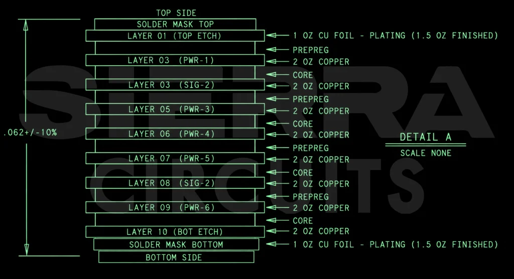
Together, these documents define the layer sequence, copper weights, dielectric thicknesses, materials, and other specifications required during fabrication. Providing this information in a consistent format helps fabricators interpret the design accurately and minimizes the risk of miscommunication during production.
In this design guide, you’ll learn how to prepare layer detail tables, create stack-up cross-sections, and document information in fab notes. It explains what each representation is used for and the information it should include. Clear and complete documentation helps manufacturers accurately interpret your stack-up and fabricate the board as intended.
What DFM guidelines should you follow when building a stack-up?
A manufacturable stack-up is essential for preventing board deformation, routing issues, and manufacturing delays.
This guide covers key DFM considerations, including:
- Maintaining a balanced stack-up,
- Selecting manufacturable via aspect ratios,
- Providing complete controlled-impedance data
- Balancing trace width and copper thickness
- Maintaining copper balance during etching.
It also highlights the importance of working with your PCB manufacturer early in the design process to ensure the build-up meets manufacturing and reliability requirements.
What fabrication tolerances affect printed board fabrication?
Tolerances for board thickness, layer-to-layer registration, controlled impedance, bow and twist, and copper weight affect PCB stack-up construction.
These tolerances vary from one fabricator to another based on manufacturing equipment, process capabilities, and quality control standards.
Reviewing them early helps you align the design’s specifications with the manufacturer’s capabilities.
The guide explains how each tolerance affects fabrication, from variations in finished board thickness and layer alignment to impedance control and board flatness. It also covers copper weight tolerances and the factors that can cause variation during manufacturing.
Understanding these limits helps designers set realistic specifications and avoid manufacturing issues.
How is a stack-up inspected after manufacturing?
Manufacturers use cross-sectional analysis and first-article inspection (FAI) to verify that the fabricated PCB meets the specified stack-up and manufacturing requirements.
Cross-sectional analysis examines the board’s internal construction to verify layer arrangement, material and dielectric thicknesses, copper plating, vias, and layer-to-layer registration.
First-article inspection (FAI) evaluates the first manufactured board against the approved design and specifications and documents the findings in an FAI report.
These inspections confirm that the manufacturer built the completed board according to the approved design and manufacturing specifications. They help identify issues related to layer alignment, dielectric thickness, copper plating quality, and internal structural defects.
A reliable stack-up starts with getting the fundamentals right. Choose the right materials, arrange layers to ensure manufacturability and signal integrity, and clearly document fabrication requirements. Each of these aspects can affect the board’s performance, reliability, and ease of manufacturing.
Sierra Circuits’ PCB Stack-Up Design Guide brings these considerations together in one practical resource, helping you make informed stack-up decisions and communicate your requirements clearly to your CM.
Download the design guide today!