Contents
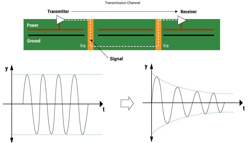
When a signal travels from the source towards the load through a PCB conductor, it experiences attenuation due to trace resistance and dielectric loss resulting in energy loss.
Signal attenuation is the most prevalent term when high-speed signals propagate on a circuit board. It is one of the primary factors responsible for signal degradation that leads to signal integrity issues.
What is signal attenuation?

Signal attenuation is the measurement of the reduction in signal strength (amplitude and intensity) when a signal propagates through a transmission medium. It is an important property in telecommunication applications because it calculates signal strength as a function of distance.
Lossless signal transfer can be achieved when the information provided at the transmitter remains the same when decoded at the receiver. Adequate threshold levels should be met to extract the correct information from the signal.

Signal Integrity eBook
6 Chapters - 53 Pages - 60 Minute ReadWhat's Inside:
- Impedance discontinuities
- Crosstalk
- Reflections, ringing, overshoot and undershoot
- Via stubs
Download Now
How is signal attenuation calculated?
Signal attenuation is estimated in decibels (dB) per unit length of the transmission medium. It can be calculated both in terms of power (Ap) and voltage (Av).
To avoid the chances of attenuation, the transmitter sends multiple signals to ensure at least one signal reaches the final destination which is the receiver. But this practice reduces the overall network speed due to the requirement of those extra signals being sent.
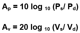
Where:
Ps is the signal power at the source
Pd is the signal power at the load
Vs is the signal voltage at the source
Vd is the signal voltage at the load
The lower the attenuation, the higher the efficiency of the transmission medium. Higher attenuation means there is more signal loss and decreased amplitude at the receiver side.
Attenuation factor or attenuation coefficient
The attenuation factor determines the distance up to which a signal can travel and still provides adequate data bits or information. It quantifies different transmission mediums based on how the transmitted signal’s amplitude decreases with frequency. It is given by:
AF = Pout/Pin
Signal attenuation factor depends upon:
- Length of the transmission medium
- Material of the transfer medium
- Physical conditions
Signal attenuation in a transmission line
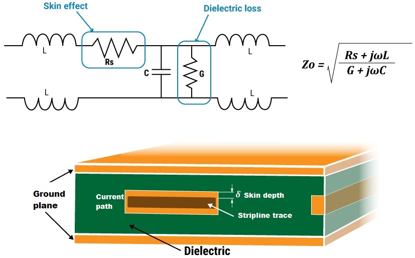
In a transmission line, attenuation loss is the amalgamation of two losses: conductor loss and dielectric loss. The conductor losses are due to the presence of imperfect conductivity and resistance of the traces, while dielectric losses exist due to the dielectric material.
The signal attenuation factor of a transmission line of length ‘l’ is given by:
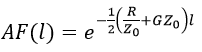
In dBs, signal attenuation is expressed as:
It can also be expressed as dB loss per unit length, which is:
Note: Ignore the minus sign, keeping in mind that it is a dB loss.
The above equation is representing total insertion loss per unit length of the transmission line and written as:
R/Z0 is the loss component that is proportional to R, the resistance of the trace per unit length, and is called the conductor loss. It is denoted by αC. The component GZ0 is proportional to G – the conductance of the dielectric material and is called the dielectric loss. It is represented by αd.
![]()
Also, read our post on losses in PCB transmission lines.
The dielectric losses are negligible in comparison to conductor losses. Up to 20GHz, the loss tangent associated with PCB materials (i.e., FR4) does not change appreciably. This is the primary cause for the dielectric loss curve in being almost a flat line with frequency. The distance between a transmitter and receiver is generally less than 1m in a PCB. So, the dielectric losses can be assumed constant over the frequencies. Being the sum of conductive loss and dielectric loss, the total loss is dominated by conductive losses.
FR4 material used in circuit board design has a loss tangent of the order of 0.003.
Why does the signal attenuate when it reaches the trace end?
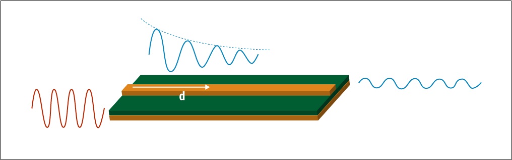
The amplitude of a signal is distorted by the trace resistance and the dissipation factor of the board’s dielectric. The effect is more prominent at high frequencies since signals tend to travel along the surface of traces. Attenuation leads to slow signal rise times and increases the possibility of data errors.
A high-frequency transmission channel makes it difficult for the receiver to interpret the actual information. The following transmission losses take place due to transmission medium effects:
- Dielectric absorption: The dielectric material absorbs signal energy when a high-frequency signal travels on the board surface. It reduces the signal intensity that can only be controlled by choosing a perfect PCB material. Pick a material with a low-loss tangent for less dielectric absorption.
To learn more about material selection read PCB material selection: electrical and manufacturing considerations.
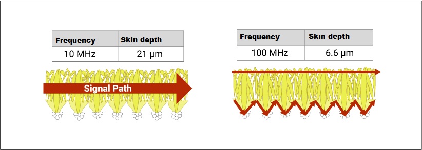
- Skin effect: Skin effect is a phenomenon due to which higher frequency components start traveling closer to the outside of a circuit board conductor rather than within it. High-frequency signals are also responsible for generating waveforms with varying current values. Such signals have their self-inductance values, which initiate an increased inductive reactance as frequency increases. It is responsible for the conductive area reduction on the PCB surface, leading to more resistance and attenuation in the signal amplitude. The skin effect can be reduced by increasing the trace width (surface area) but it is not always feasible because changing trace geometry may lead to impedance issues.

What causes signal attenuation in a PCB?
As the signal range increases, attenuation also increases. The below-listed factors are responsible for signal attenuation:
- Noise sources: RF frequencies, leakage currents, and electrical currents interfere with the signal leading to attenuation. More noise, more attenuation!
- Distance between transmitter and receiver: When a signal traverses longer distances, its strength decreases. The more the distance between two points, the higher the attenuation.
- Trace width: A signal suffers less attenuation when it travels through a wider trace.
- Crosstalk: Crosstalk in nearby traces in nearby traces is also responsible for signal attenuation.
- Conductors and connectors: When a signal passes through different conductive materials and connector surfaces, it suffers attenuation.
- Frequency of transmission: Radio waves with a shorter wavelength have a larger attenuation. Such signals are transmitted via 2.4GHz or 5GHz electromagnetic waves. Electromagnetic waves have high frequencies and short wavelengths. Therefore, radio signals have large attenuation and cannot traverse long distances.
- Resistive losses associated with conductor material: Conductive material like copper used in the manufacturing of transmission lines introduces resistive losses, resulting in attenuation of the signals propagating in copper traces.
- Losses associated with dielectric material: Losses in dielectric materials sandwiched between the transmission lines introduce dielectric losses. This dielectric loss forms a conductance, also called inverse resistance, across the substrate and absorbs part of the propagating signal energy leading to signal degradation.
- Copper surface roughness: Copper surface roughness on a PCB also acts as a resistance to signal propagation. Rough copper traces increase the resistance because the topography of the copper surface moves the signal up and down. Surface spikes can create an increase in capacitance, as well. Smooth copper is the solution to this problem but costs more.

- Resistance of ground return path: As frequency increases, the ground return path becomes narrow and uses less copper area, resulting in increased resistance.
Also read, how to reduce parasitic capacitance in PCB layout?
How do you reduce signal attenuation?
Signal attenuation can be mitigated by adopting the below-mentioned techniques:
- Make use of repeaters: If the received signal is weak, then a repeater is used to regenerate the original signal by reducing attenuation. It also enhances the range of the signal so that it could travel longer distances without fail.
- Make use of amplifiers: If the received signal is weak, then an amplifier is used to increase its amplitude, unlike a repeater that regenerates the whole signal.
- Right material choice: Careful selection of low-loss dielectric materials and low resistance traces can minimize signal attenuation.
- Use programmable differential output voltages (VOD) settings: Programmable VOD ensures that the drive strength is in synchronization with the line impedance and the length of the trace. Increasing the VOD at the driver enhances the signal at the receiver.
- Pre-emphasis: Boosting signal strength using an amplifier is not the only solution for attenuation control because it also amplifies the associated signal noise and jitter. Pre-emphasis only strengthens the high-frequency components of the signal by increasing the level of the first transmitted symbol. The subsequent symbol levels remain untouched if they are transmitted at the same level. For instance, if a signal transmits a high level for three symbols, only the first symbol is strengthened. The next two symbols will be transmitted at the usual level.
6. Receiver equalization: When a signal reaches the receiver, an equalization circuitry attenuates the low-frequency components of the signal to recover for the transmission line losses.
Here’s what Syed Ubaid Ali Warsi, Owner of Wavetroniks, has to say about high-speed and HDI PCB design strategies.
Signal attenuation measurement using a VNA
A vector network analyzer (VNA) is used to perform frequency domain analysis thus attenuation analysis also. It has a high dynamic range and is very useful in identifying the actual cause of a signal integrity problem. In other words, it is an excellent test and measurement tool for understanding what is causing eye closure in high data rate systems.
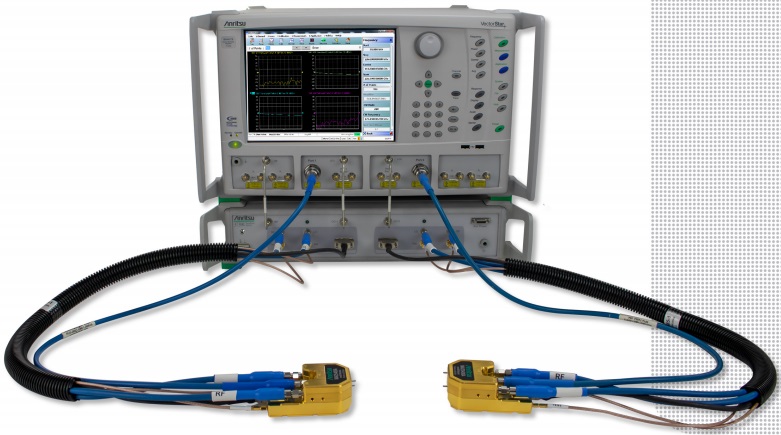
With wide frequency bandwidths, a VNA allows channel characterization that can be as broad as 70kHz to 145GHz. This wide bandwidth enables building accurate models by including multiple harmonics and providing a low-end frequency for better DC extrapolation. It also offers accurate resolution in the time domain for locating defects in the channel. A VNA equipment is beneficial in understanding the physical structures and their imperfections.
For example, for a printed circuit board, VNAs are suitable for analyzing real-world channel defects, like exceeding tolerances on PCB artwork, plating, and dielectric thickness variations. They can be used to evaluate connector performance, construction, and how well they are mounted. They can also be used to analyze multilayer PCB stack-ups and find imperfect vias or ground plane issues.
Also, most signal integrity channels use test fixtures during characterization. VNAs have an excellent capability of evaluating the impacts of these fixtures. Network extraction produces a model that is used to reduce the effect of these fixtures. De-embedding is the process of applying the model to subsidize the effects of fixtures on the calculated results.
Signal attenuation is a result of trace/conductor resistance and associated dielectric losses, which increase by longer distances and higher frequencies. It can be reduced by improving the dielectric properties of the PCB substrate material and increasing the conductor’s size. Attenuation control can help designers to realize a PCB that can work seamlessly at a high frequency. The board traces possess losses that can have a small or significant effect on a propagating high-speed digital signal.
Signal and Plane Layer Estimator for high-speed boards
Estimating the number of optimum signal layers is a crucial step in any PCB design. The stake goes higher when it comes to high-speed circuit boards as they are prone to EMI. To address this pain point, we have introduced the Signal Layer Estimator that assists you in the design and development stages.
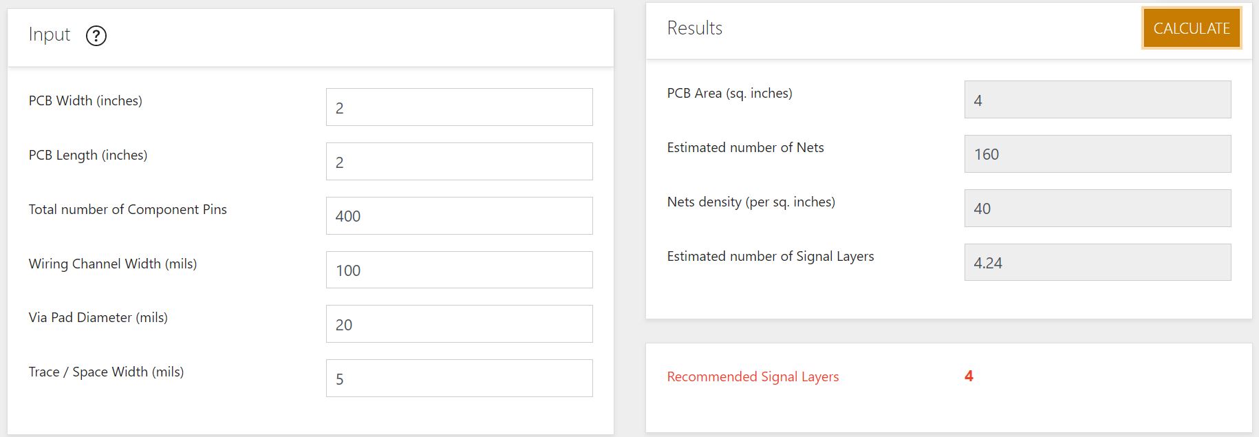
This calculator not only provides the number of recommended signal layers but also assists you with PCB area, number of nets, and net density. You’ll have to input the following parameters and click on Calculate to view the results:
- PCB width
- PCB length
- Total number of component pins
- Wiring channel width
- Via pad diameter
- Trace/space width
Let us know in the comments if you would like to read about any specific topic in our blog. If you are a PCB designer who deals with high-speed boards then our design guide below can help you with your designs.

High-Speed PCB Design Guide
8 Chapters - 115 Pages - 150 Minute ReadWhat's Inside:
- Explanations of signal integrity issues
- Understanding transmission lines and controlled impedance
- Selection process of high-speed PCB materials
- High-speed layout guidelines
Download Now