Organic solderability preservative (OSP) is a cost-effective, ultra-flat PCB surface finish ideal for high-volume consumer electronics, HDI layouts, and nickel-sensitive applications. It performs best when boards move quickly from fabrication to assembly.
The protective layer forms an ultra-thin organic coating directly on copper, preserving pad flatness and enabling reliable soldering without additional metal buildup.
Typical metallic finishes add multiple metal layers on top of copper, which can increase cost and process complexity.
In this article, you’ll learn the OSP coating’s composition, when to select OSP surface finish, and what to include in your fabrication notes.
Highlights:
- OSP is best suited for cost-sensitive, high-volume consumer and automotive electronics.
- The organic coating layer decomposes during reflow, allowing solder to bond directly to the copper layer.
- The water-based, lead-free process makes it an environment-friendly finish.
What is OSP PCB surface finish?
Organic solderability preservative is a lead-free, RoHS-compliant non-metallic coating applied to bare copper features to prevent oxidation during assembly and storage. The protective layer decomposes during reflow and allows molten solder to bond directly to the copper pads.
It is widely used in consumer electronics, automotive applications, and high-volume PCB manufacturing due to its low cost and flat surface profile.
Composition of organic solderability preservative coating
The protective layer is made from azole-based organic compounds (typically benzotriazoles, imidazoles, and benzimidazoles). It is applied as an ultra-thin film approximately 0.20 – 0.50 µm thick.
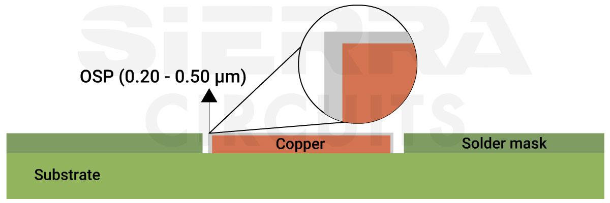
These compounds adsorb onto copper through coordination bonding, forming copper-OSP complexes across the pad surface.
- Benzotriazole forms thinner films with excellent solderability.
- Imidazole forms thicker films with improved oxidation resistance and shelf life.
The selected chemistry directly influences film thickness, durability, reflow endurance, and storage performance.
IPC-4552 defines the thickness requirements, thermal stability, and solderability performance for this finish.
If your board requires OSP coating, specify it clearly in your PCB fabrication notes along with storage and assembly requirements.
When to choose OSP
OSP is a practical choice for low-cost designs with ultra-flat surface requirements.
It is ideal for:
- Fine-pitch and HDI designs where flatness is critical (≤0.5 mm pitch).
- Cost-sensitive, high-volume PCBs that are assembled shortly after fabrication.
- Magnetic-sensitive applications, such as medtech equipment, where nickel is undesirable.
Select this protective coating only when storage time, handling, and assembly schedules can be tightly controlled.
When to avoid OSP
It is not recommended for:
- Gold fingers or plug-in contacts.
- Wire-bonding pads.
- PCBs that require long-term storage.
Choose ENIG in these cases.
Why OSP surface finish for your PCB designs?
OSP coating is a low-cost and eco-friendly surface finish with excellent solderability. Here are the benefits of choosing the organic coating:
- Excellent solderability preserves good wetting and solder joint formation for both reflow and hand soldering.
- Lower cost than most metallic PCB surface finishes.
- Environmental-friendly due to water-based process with low-toxicity effluents and minimal chemical waste.
- Absence of metals ensures excellent coplanarity for fine-pitch components and BGAs.
- Direct copper interface eliminates nickel-related losses in high-frequency designs.
- Fast fabrication turnaround due to simple chemistry.
- Lead-free and RoHS-compliant.
- No black pad risk, as no nickel layer is present.
Limitations:
- Limited shelf life (typically 6-12 months).
- Oxidizes if mishandled.
- Low abrasion resistance.
- Difficult to inspect.
- Low copper adhesion strength compared to metallic finishes.
- Sensitive to moisture at high humidity.
- Limited tolerance for multiple reflows.
Things to include in your fab notes about OSP coatings
- IPC standard to consider (IPC-4552).
- Maximum shelf life (e.g., 9 months).
- Storage requirements if the board is humidity-sensitive.
- Solderability testing requirements if storage exceeds the specified shelf life.
- Alternate coatings (ENIG or immersion tin), if applicable.
For more, download the PCB Fab and Assembly Notes for PCB Designers.

PCB Fab and Assembly Notes for Designers
8 Chapters - 72 Pages - 70 Minute ReadWhat's Inside:
- Guidance on how to write comprehensive fab documentation
- Advanced fabrication notes for flex, rigid-flex, and hybrid stack-ups
- Difference between fabrication and assembly notes
- Assembly documentation essentials: BOM, X-Y data, and drawings
Download Now
How OSP protects copper features from oxidation
The coating reacts with the top atomic layers of copper to form copper-organic complexes. This thin barrier prevents oxygen and humidity from reaching the copper surface.
Over time, protection diminishes due to:
- Exposure to air
- Thermal cycling and solder reflow
OSP is also sensitive to abrasion during handling.
Its shelf life depends on coating thickness and storage conditions, but typically ranges from 6 to 12 months under ideal conditions (20 – 25°C, 45 – 55% RH).
Need circuit boards within a quick turnaround time?
Talk to a PCB expert: Book a meeting or call us at +1 (800) 763-7503.
Sustenance of organic solderability preservative during reflow cycles
During reflow soldering, the organic coating thermally decomposes and volatilizes, exposing clean copper for solder wetting. Flux removes residual oxides, allowing solder to bond directly to copper pads.
As solder reacts with copper, intermetallic compounds form 2 layers:
- Layer 1: Cu₆Sn₅ (intermetallic compound at the solder interface).
- Layer 2: Cu₃Sn (forms closer to the copper base over time).
Since no nickel barrier is present, the protective layer provides low electrical resistance and excellent solder wetting when handled correctly.
The coating typically survives 4 – 6 reflow cycles, but solderability degrades with excessive rework. Opt for metallic finishes for boards requiring many reflows.
OSP vs. HASL vs. ENIG
| Feature | Organic solderability preservative (OSP) | Hot air solder leveling (HASL) | Electroless nickel immersion gold (ENIG) |
|---|---|---|---|
| Finish type | Organic, non-metallic | Metallic | Metallic |
| Coating thickness | Very thin (0.2 – 0.5 µm) | Thick and uneven (~3 – 12 µm) | Moderate, controlled (nickel: 2.54 to 6.35 µm, gold: 0.0508 to 0.2032 µm) |
| Surface flatness | Excellent, extremely flat | Moderate, uneven surface | Excellent, flat |
| Solderability | Very good | Excellent | Excellent |
| Shelf life | Limited (6 – 12 months) | Long | Very long |
| Reflow capability | Limited (~4 – 6 cycles) | Multiple reflows | Multiple reflows |
| Handling sensitivity | High (sensitive to fingerprints and moisture) | Low | Low |
| Durability | Low | High | Very high |
| Fine-pitch/BGA support | Excellent | Limited | Excellent |
| Wire bonding | Not supported | Not supported | Supported |
| Environmental impact | Very low: water-based, RoHS-compliant | Moderate | Moderate |
| Inspection difficulty | High (transparent coating) | Low | Low |
| Typical applications | High-volume consumer electronics and medical applications | General-purpose PCBs (not recommended for SMT) | Aerospace, high-reliability, high-speed, and microwave boards |
| Relative cost | Low | Low – medium | High |
For more on HASL, read HASL surface finish.
Step-by-step OSP surface finish application process
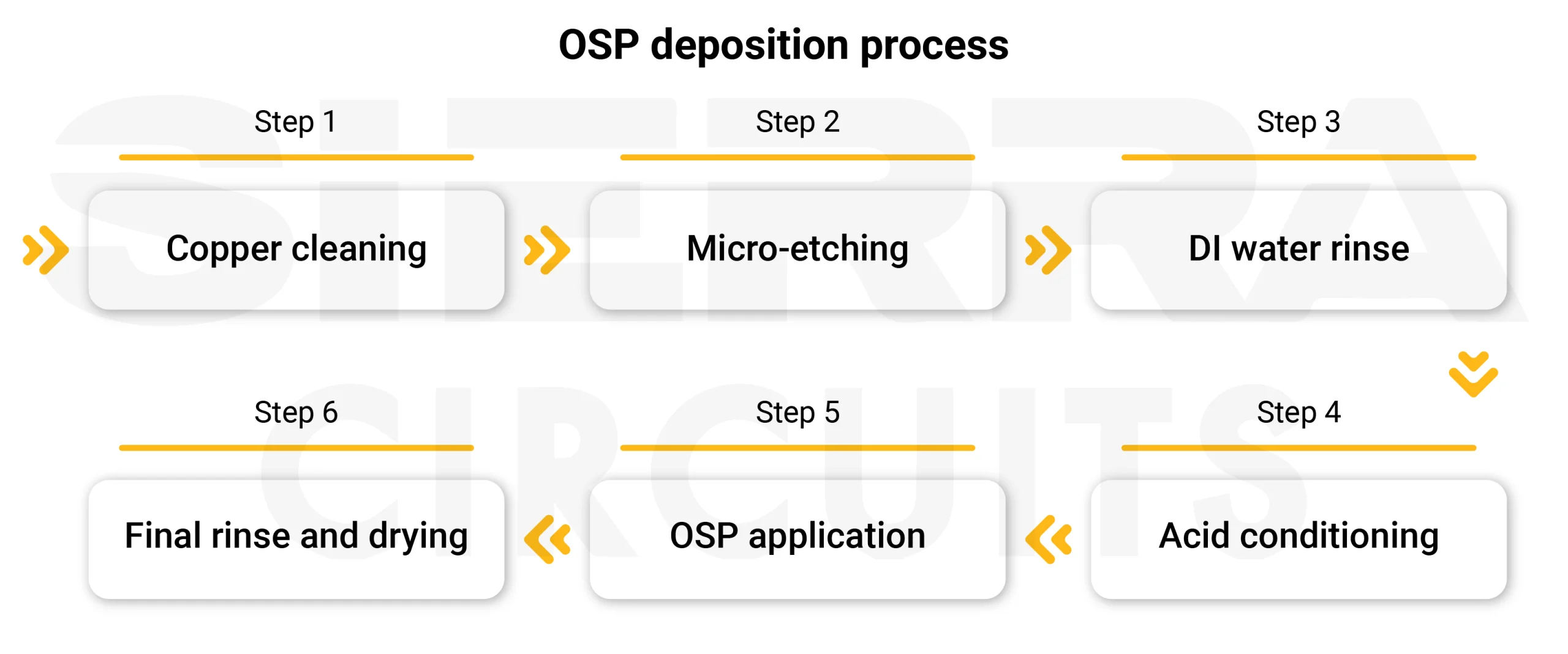
Step 1: Copper cleaning
Alkaline cleaners remove oils, fingerprints, oxidation films, and organic residues on the bare board. This step is crucial to avoid uneven OSP thickness and degraded solderability.
Step 2: Micro-etching (topography enhancement)
Micro-etching removes surface oxides and slightly roughens the copper to improve bonding with the OSP coating, with a typical copper removal of around 0.2 µm.
Step 3: DI water rinse
Deionized water rinsing prevents ionic contamination that can cause tarnishing after reflow soldering.
Step 4: Acid conditioning
A mild acid dip stabilizes surface chemistry and prepares copper for uniform coating.
Step 5: OSP application
The PCB is immersed in the organic solderability preservative solution. Organic molecules chemically bond to copper atoms, forming a thin, conformal protective film.
Step 6: Final rinse and drying
A final DI rinse (typically mildly acidic, ~pH 4 – 5) removes excess chemicals, followed by controlled drying.
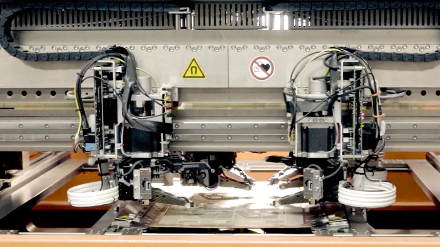
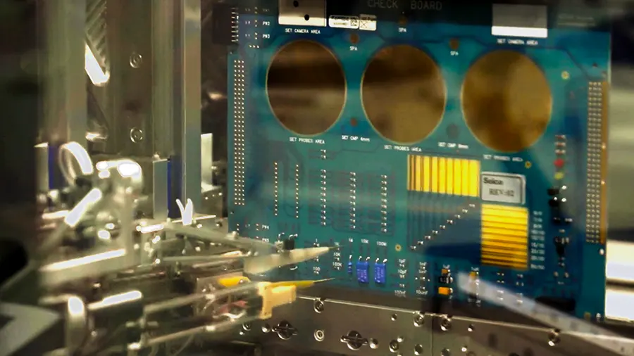
Sierra Circuits fabricates high-quality PCBs using advanced technologies such as X-ray drill machines, mechanical vision drilling systems, and Seica flying probe test machines.
Visit our rigid PCB manufacturing capabilities to learn more.
OSP surface finish is a cost-effective, copper-direct protective layer optimized for high-volume manufacturing and fine-pitch assemblies.
The coating lacks the durability and wire-bonding capability of premium finishes like ENIG or EPIG, but its low cost, excellent flatness, and strong solderability make it a preferred choice for consumer and automotive electronics.
