PCB Fab and Assembly Notes for Designers
Sierra Circuits’ PCB Fab and Assembly Notes for Designers helps you create efficient fabrication and assembly documentation.


The PCB Fab and Assembly Notes guide helps you communicate your design intent effectively. It clearly specifies what to include in fabrication drawings, stack-up, assembly files, and bill of materials (BOM).
Here’s a quick breakdown of what you’ll learn:
- Why fabrication and assembly notes are critical for successful printed circuit board manufacturing
- The information every manufacturer expects to see in fabrication notes
- How to specify stack-ups, drill requirements, materials, tolerances, and surface finishes
- Best practices for documenting advanced fabrication requirements such as rigid-flex boards, hybrid stack-ups, and embedded components
- Essential assembly documentation, including assembly drawings, BOMs, pick-and-place files, and netlists
- What assembly technicians need to place, solder, and inspect components correctly
- BOM management strategies, including handling alternate parts and DNP/DNI components
- Additional documentation required for complex assemblies, including fiducials, tooling holes, panelization, conformal coating, and underfill
- Practical guidelines for writing clear, complete, and manufacturer-friendly fabrication and assembly notes
The following sections will provide you with a closer look at each of these topics.
How to write effective fabrication and assembly notes?
Fabrication and assembly notes should give manufacturers clear, unambiguous instructions for building your PCB. Document critical requirements directly in the documentation rather than relying on assumptions or information scattered across different files.
Use clear and consistent terminology for materials, dimensions, tolerances, finishes, assembly processes, and special features. Make sure drawings, BOMs, pick-and-place files, and other manufacturing files are aligned with the same design revision. If a requirement applies only to a specific area or feature, clearly identify its location and any applicable exceptions.
Before releasing the design, review the complete documentation package to ensure all required files are included and accurate. Well-organized notes reduce back-and-forth communication with your CM, prevent manufacturing errors, and ensure the finished PCB matches your design intent.
Why are fabrication notes important?
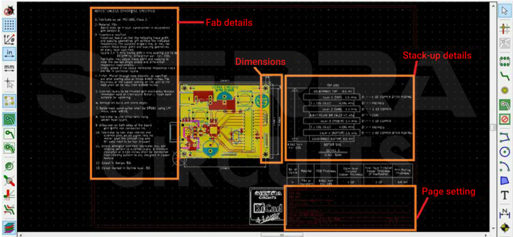
PCB fab and assembly notes communicate manufacturing requirements that Gerber/ODB++/IPC-2581 and CAD data alone cannot convey. They provide fabricators with the information needed to manufacture your boards according to their electrical, mechanical, and reliability requirements.
This document helps you clearly document critical manufacturing requirements, including dielectric materials, stack-up details, drill tolerances, surface finishes, manufacturing standards, and other process specifications. By documenting these requirements, you reduce production ambiguity, minimize engineering queries, and ensure the finished board matches your original design intent.
Fabrication drawings provide the graphical representation of circuit boards. They should define the board outline, drilled holes, cutouts, stack-up, tooling holes, and other mechanical features. Fabrication drawings create a complete manufacturing package that serves as references for production, inspection, and future revisions.
Manufacturers rely on several production files to interpret your design accurately. Standard design outputs such as Gerber files, ODB++, or IPC-2581 provide the layer information, while drill files, stack-up data, netlists, and stencil files specify the remaining manufacturing details.
What should you include in fabrication notes?
It should include stack-up details, drill specifications, board dimensions, surface finishes, via treatments, manufacturing tolerances, testing requirements, and packaging instructions that guide fabricators throughout the production process.
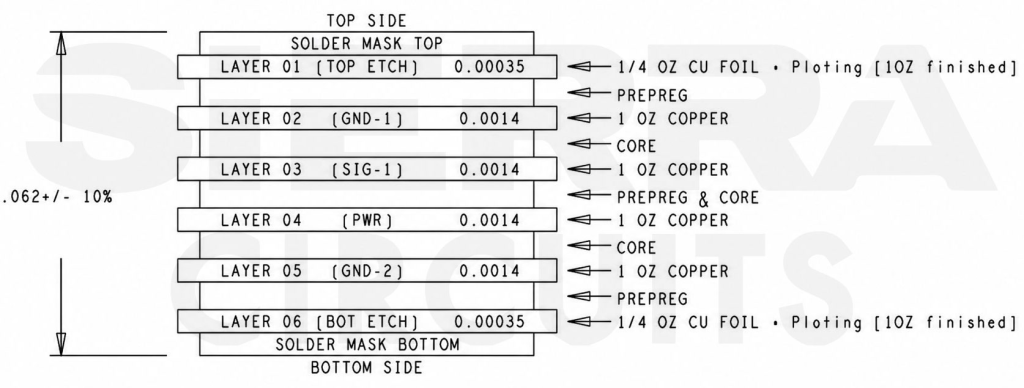
A complete stack-up specification is one of the most important elements of your fabrication notes. Clearly define the layer sequence, dielectric materials, copper weights, and finished board thickness. For controlled impedance designs, include the target impedance values, dielectric properties, and trace geometries required to achieve consistent electrical performance.
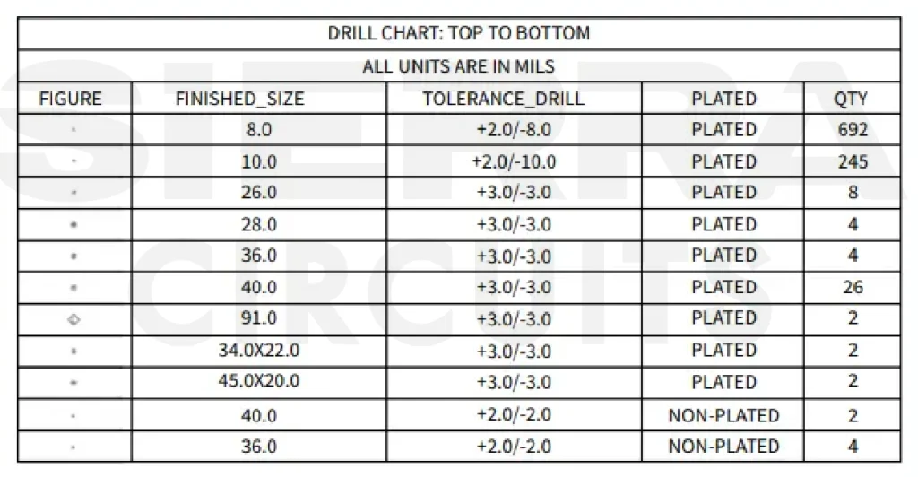
Document drill information in detail to ensure mechanical accuracy and reliable interconnections. Include finished hole sizes, plated and non-plated holes, drill tolerances, blind and buried vias, back-drilling requirements, and any sequential lamination instructions. A comprehensive drill chart reduces interpretation errors and helps manufacturers produce every drilled feature within specification. An example of a drill chart is shown below.
Define board dimensions, routed slots, internal cutouts, tooling holes, fiducials, and hole-to-edge clearances in the fabrication drawing. If your design includes non-standard outlines, cavities, or other special mechanical features, provide the necessary dimensions and tolerances. This eliminates uncertainty during machining.
Your fabrication notes should also identify the required surface finish and via processing methods. Specify whether the board requires ENIG, ENEPIG, HASL, immersion silver, or another finish. This helps the printed circuit board meet its solderability, durability, and performance objectives. Likewise, specify the required via, such as tenting, plugging, filling, or via-in-pad structures, to support the intended assembly process.
Finally, establish the manufacturing quality requirements by defining applicable IPC standards, dimensional tolerances, electrical testing methods, inspection criteria, and packaging instructions. Including these details helps manufacturers verify board quality before shipment while ensuring the finished product satisfies your design and reliability expectations.
How do advanced fabrication notes improve manufacturability?
Specifying advanced fabrication requirements helps manufacturers accurately build complex board designs. These specifications provide additional guidance for designs with non-standard stack-ups, mixed materials, flexible circuits, and other specialized PCB features.
Cross-sectional drawings are particularly useful for multilayer printed circuit boards. They illustrate the layer sequence, material thicknesses, via structures, and controlled-impedance features. This visual reference helps fabricators interpret complex stack-ups accurately and minimize manufacturing errors.
For rigid-flex and hybrid designs, fabrication notes should clearly define flex regions, bend radii, material combinations, and bonding requirements. Providing these details ensures that the finished circuit board meets its electrical and mechanical performance requirements while reducing the risk of potential issues such as delamination and premature failure.
Designs that include embedded components, cavities, castellated holes, countersinks, or wire-bonding pads also require additional documentation. Specifying their locations, dimensions, tolerances, and processing requirements gives manufacturers the information needed to fabricate these features accurately and reduces the need for clarification during production.
What is PCB assembly documentation?
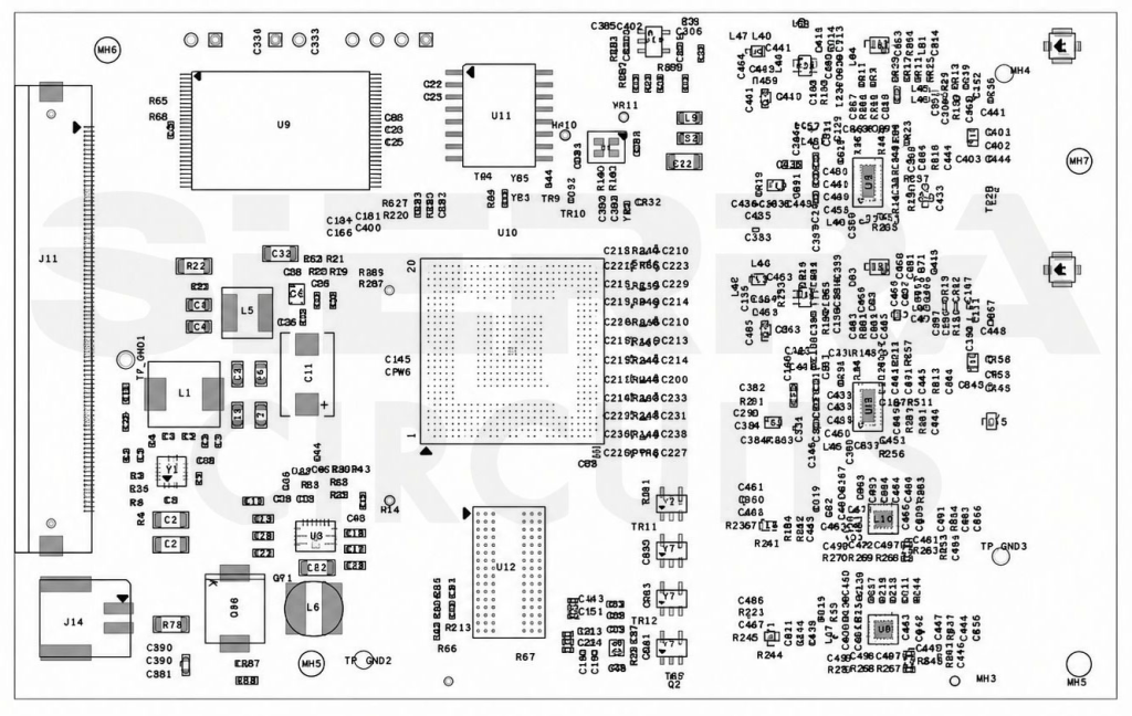
PCB assembly documentation consists of the files and instructions manufacturers use to place, solder, inspect, and verify components on a fabricated circuit board. Assembly notes explain how components should be mounted, oriented, and handled during production, while supporting documents provide the information needed for procurement, automated placement, and quality control. Together, these documents communicate assembly-specific requirements that may not be defined in the circuit layout or manufacturing files.
Fabrication documentation focuses on building the bare board, while assembly documentation guides the population of components onto the fabricated board. Together, they provide manufacturers with the information needed to produce a complete PCB assembly that functions as intended.
A complete assembly package typically includes assembly drawings, a bill of materials, pick-and-place files, and a netlist. Assembly drawings identify component locations and orientations, the BOM specifies the required parts, pick-and-place files provide placement coordinates for automated equipment, and the netlist verifies electrical connectivity during testing.
Before submitting your design for assembly, verify that all required files are complete, correctly formatted, and included in the documentation package. A final submission check helps prevent missing data, reduce production delays, and enable your contract manufacturer to begin assembly without unnecessary clarification.
What should your assembly notes communicate?
Assembly notes should provide clear instructions for component placement, soldering, inspection, and handling so manufacturers can assemble each PCB as intended. They communicate design-specific requirements that assembly files alone may not convey. This helps you reduce rework and improve production consistency.
Start by documenting component orientation, polarity, and reference designators to ensure polarized devices and integrated circuits are installed correctly. Include mounting requirements, component clearances, and any special placement instructions to prevent mechanical interference and simplify inspection.
Assembly notes should also define soldering requirements, including acceptable processes, temperature limitations, and any instructions for lead-free or high-temperature assemblies. If the design must comply with standards such as RoHS or REACH, clearly specify these requirements to ensure the appropriate materials and manufacturing processes are used.
Finally, communicate inspection and testing requirements, along with any cautionary markings or handling instructions for sensitive components. Complete assembly notes help manufacturers assemble, inspect, and verify the finished board accurately, minimizing manufacturing errors and ensuring consistent product quality.
What should your bill of materials include?
A well-structured BOM should identify every component required to assemble your PCB, along with the information needed to source the correct parts. A complete material list reduces procurement issues and provides assemblers with a single reference for part selection.
Beyond part numbers and quantities, include manufacturer names, approved vendor information, package types, electrical values, and reference designators. Consistent naming and formatting make it easier to verify components before assembly and reduce the risk of sourcing incorrect or obsolete parts.
If certain parts are designated as do not install (DNI) or do not populate (DNP), mark them clearly to prevent them from being placed during assembly. Specify approved alternate part numbers to provide additional sourcing flexibility when preferred parts are unavailable. This helps production continue without compromising design requirements.
What advanced assembly documentation should you provide?
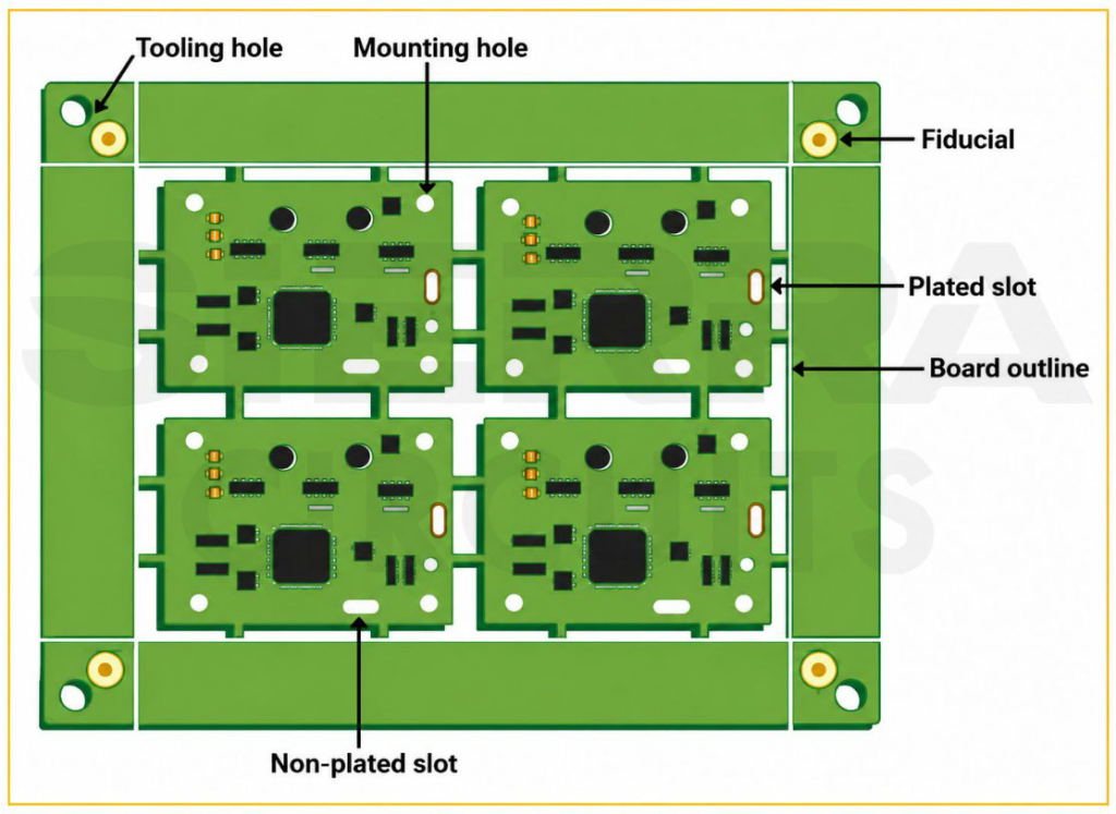
Include fiducials, tooling holes, alignment marks, panelization instructions, and any special processing requirements needed to assemble your PCB accurately. These details support automated manufacturing and communicate requirements that extend beyond standard assembly files.
Fiducials, tooling holes, and alignment marks provide reference features that help assembly equipment position the board and components accurately throughout the production process. For panelized designs, include panel layouts, breakaway tab locations, and depanelization instructions to ensure boards can be assembled efficiently and separated without damage.
If your printed board requires additional processing after component placement, document those requirements clearly. For conformal coating, specify the areas to be coated or protected. For underfill and stiffeners, specify the required materials, application locations, and process requirements. Providing these details helps manufacturers complete specialized assembly operations correctly and consistently.
Download the PCB Fab and Assembly Notes Handbook to learn practical techniques for preparing comprehensive fabrication and assembly documentation that helps reduce manufacturing issues and supports a successful first build.