


Contents

On-demand webinar
How Good is My Shield? An Introduction to Transfer Impedance and Shielding Effectiveness
by Karen Burnham
PCB ringing is an unwanted oscillation of voltage or current in a circuit board. During the signal transition from low to high or high to low, the voltage doesn’t immediately stabilize at the desired level; instead, it oscillates briefly before settling down. This oscillation creates a series of voltage spikes, resembling a ringing pattern on the signal waveform.
Highlights:
- Implementing a damping resistor at the source end, properly terminating the signal lines, and maintaining uniform trace width are some of the ways to minimize ringing.
- Parasitic capacitances/inductances oscillating during high-speed signal transitions, unwanted stub lengths, and ground bounce cause transient oscillations.
- Ringing degrades signal integrity, causing distorted waveforms, timing inaccuracies, EMI/RFI emissions, noise coupling, component stress, and increased power consumption.
- Eye diagrams, TDR, and spectrum analyzers identify ringing.
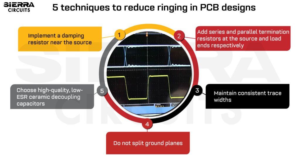
5 techniques to minimize ringing in your circuit board designs
Here’s an infographic that quickly summarizes the ways to minimize transient oscillations in your designs.

1. Add a damping resistor near the source

Achieving a critically damped state in the transmission line is crucial to achieving the fastest settling time without overshoot or oscillation. For this, you need to incorporate a damping resistor near the source. The correct choice of this resistor value is key to eliminating transient oscillations while maintaining the fastest rise time. These resistors usually have values below 100Ω, ensuring the signal reaches the desired logic level smoothly.
In this process, you can employ an RLC (resistor-inductor-capacitor) model to calculate the transient oscillation frequency and damping. By determining these parameters, you can precisely calculate the value of the series termination resistor needed to achieve critical damping:
Z= 2 √L/C
2. Effectively terminate the signal lines
Termination resistors are strategically placed to absorb reflected signals, reducing the likelihood of ringing. Properly terminated transmission lines ensure uniform impedance throughout the transmission line. In this section, we will explore two widely used termination techniques:
a. Series termination
It is a simple and effective termination scheme. A termination resistor is placed in series with the signal line at the source end. The value of the series termination resistor is chosen to match the impedance of the signal line.
It absorbs the reflected signal at the source end, preventing it from propagating through the signal line. The schematic below shows the placement of a series termination resistor at the source end.
Place the series termination resistor to match the total driver impedance to the transmission line impedance. Here’s an example of a series termination resistance calculation:
Rsource +R series termination resistor= Transmission line impedance (Z0)
If Z0 = 50Ω and, Rsource = 28Ω
then, R series termination resistor = 22Ω

b. Parallel termination
A parallel termination resistor is placed in parallel with the signal line at the load end. The value of the parallel termination resistor is also chosen to match the impedance of the signal line. The resistor absorbs the reflected signal at the load end.

For more on circuit board trace terminations, read 5 PCB trace termination techniques to reduce signal reflections.

Controlled Impedance Design Guide
6 Chapters - 56 Pages - 60 Minute ReadWhat's Inside:
- Understanding why controlled impedance is necessary
- Stack-up design guidelines
- How to design for impedance
- Common mistakes to avoid
Download Now
3. Implement short traces with uniform width
Effective routing strategies help minimize impedance mismatches, signal reflections, and subsequent ringing. In this section, we’ll look into a set of routing tips that help you reduce transient oscillations in your design:
- Keep signal traces as short as possible to lower inductance and minimize loop area and ground bounce.
- Maintain consistent trace widths to ensure controlled impedance.

- Place critical components, such as microcontrollers or high-speed ICs, close to the power source to avoid trace stubs.
- Group components of specific applications together to reduce the loop areas.
- Reduce via stub lengths by placing vias as close to component pads as possible when routing between layers.
4. Do not split the ground planes
Inconsistent ground connections can introduce voltage fluctuations, contributing to ringing in the signal. Adhere to the following techniques for an effective return path:
- Avoid splitting the ground plane, as it can induce unwanted noise.
- Implement stitching vias to connect different sections of the ground plane, ensuring uniform grounding throughout the PCB. For low-frequency designs, we recommend incorporating λ/20, and for high-frequency circuits, λ/10 spacing between stitching vias, where λ is the signal operational wavelength.

- Utilize solid ground planes on multi-layer PCBs to provide a low-impedance return path for signals.

5. Incorporate low-ESR decoupling capacitors
Choose high-quality, low-ESR (equivalent series resistance) ceramic capacitors for decoupling purposes. These decoupling capacitors are better at suppressing ringing compared to their electrolytic counterparts. Always position decoupling capacitors as close as possible to the power and ground pins of active components, such as microcontrollers, FPGAs, and ICs.
To avoid unnecessary resonant peaks, incorporate multiple capacitors of identical value in parallel to the power supply. If your design requires capacitors of different values, position the lowest-value capacitor closest to the power supply (as shown in the image).

Key takeaways:
- You can achieve critical damping by adding a series damping resistor near the source, calculated using an RLC model.
- Implement series, and parallel termination methods to match signal line impedance and nullify reflected signals.
- Keep signal traces short, maintain consistent widths, place critical components close to the power source, and reduce stub lengths.
- Minimize ground loops, use ground plane stitching vias, and ensure a continuous ground plane without splits.
- Choose high-quality, low-ESR ceramic capacitors, position them close to power and ground pins, and use multiple capacitors in parallel to avoid resonant peaks.

High-Speed PCB Design Guide
8 Chapters - 115 Pages - 150 Minute ReadWhat's Inside:
- Explanations of signal integrity issues
- Understanding transmission lines and controlled impedance
- Selection process of high-speed PCB materials
- High-speed layout guidelines
Download Now
How to detect ringing/transient oscillations in circuit designs
Detecting ringing in PCB design requires a combination of careful design practices and the use of specialized tools to analyze signal waveforms. Here are the steps and methods you can use to detect ringing in PCB design:
1. Eye diagrams determine signal distortions
An eye diagram in PCB design is a graphical representation of signal quality that can reveal ringing and other signal integrity issues. Use an oscilloscope to generate eye diagrams to visualize signal behavior over time.
Ringing spikes can be seen on an eye diagram. These fluctuations can result in narrowing eye-openings horizontally. As a result, the signal exceeds its desired voltage and current levels and makes it difficult to distinguish the valid signal levels. The simulation screenshots below show the eye diagrams without and with signal ripples.


To generate eye diagrams, the oscilloscope must have the following capabilities:
- A bandwidth that is greater than the bit rate of the signal being tested.
- A trigger that can be synchronized to the signal being tested.
- A persistence mode that allows multiple cycles of the signal to be superimposed on the screen.
Here’s how an eye diagram analyzes signal integrity in your designs:

2. TDR detects impedance discontinuity
Time-domain reflectometry instruments can measure impedance mismatches, reflections, and signal discontinuities along transmission lines. By examining TDR graphs, you can identify locations where ringing may occur due to impedance mismatches.

A TDR works by sending a pulse down a transmission line and then measuring the reflected signal. The reflected signal will vary depending on the load impedance at the line end. If the load impedance matches the impedance of the transmission line, then there will be no reflection. However, if there is an impedance mismatch, then some of the signal will be reflected back down the source, causing ringing. Also, the reflection’s direction (positive or negative) depends on whether the impedance causing the ringing is inductive or capacitive.
Peaks indicating values greater than the characteristic impedance are due to inductive effects, while signal peaks smaller than the characteristic impedance suggest capacitive effects.

Here are some tips for using a TDR instrument to identify ringing in PCB designs:
- Calibrate the TDR instrument before using it.
- Connect the TDR instrument to the PCB at the point where the signal enters the PCB.
- Set the TDR instrument to the correct impedance.
- Send a pulse down the transmission line and measure the reflected signal.
- Analyze the TDR trace to identify the location and severity of any impedance mismatches.
3. Frequency domain analysis using spectrum analyzer
A spectrum analyzer works by dividing the signal into a series of narrow frequency bands and then measuring the power in each band. It displays the results on a graph with frequency on the horizontal axis and amplitude on the vertical axis.

A series of peaks at high frequencies in the spectrum analyzer are the harmonics of the signal. By analyzing the spectrum analyzer display, you can identify the presence of ringing and determine the fundamental frequency of the ringing signal.

Here are some tips for using a spectrum analyzer to identify ringing in PCB designs:
- Use a spectrum analyzer with a bandwidth that is greater than the bit rate of the signal being tested.
- Set the spectrum analyzer to the correct frequency range.
- Connect the spectrum analyzer at the point where the signal exits the PCB.
- Send the signal through the circuit and measure the spectrum of the signal.
- Analyze the spectrum analyzer display to identify any spikes at high frequencies.
4. Sierra Circuits’ Transmission Line Reflection Calculator
Sierra Circuits’ Transmission Line Reflection Calculator will greatly help you comprehend signal characteristics in the design phase. This tool visually illustrates signal ringing at the transmission line’s source and load.

Upon entering the input parameters, click “Calculate” to generate a voltage versus time graph. The tool presents signal reflections at the input and output terminals of the transmission line through distinctive red and green curves.

Key takeaway points:
- Utilize oscilloscopes to generate eye diagrams, visualize signal behavior, and detect ringing.
- Use TDR with sufficient bandwidth to measure impedance mismatches and reflections in transmission lines.
- Employ spectrum analyzers with suitable bandwidth to detect high-frequency spikes and analyze these spikes to identify ringing in PCBs.
- Sierra Circuits’ Transmission Line Reflection Calculator facilitates a graphical representation of reflection and ringing in your PCB design.
What causes ringing in PCBs?
1. Impedance discontinuities in transmission lines
When a signal encounters a sudden change in impedance, such as at the end of a transmission line that is not properly terminated, it can cause a reflection. Reflections can cause ringing because they superimpose on the original signal.
2. Faster switching speed increases parasitic effects
The parasitic capacitances and inductances in a circuit act like a tank circuit, which is a resonant circuit that can oscillate at a certain frequency. When the signal switches rapidly, it excites the tank circuit, causing it to oscillate. This oscillation results in the signal ringing.
The faster the signal switches, the more pronounced the ringing can become. This is because the tank circuit has less time to settle before the signal switches again. In addition, high-speed digital circuits often use long traces with complex geometries. This can increase the amount of parasitic effects in the circuit.
3. Unwanted stub length leading to signal reflection
A stub is a short length of transmission line that is not terminated in a load. When a signal encounters a trace or via stub, it will be partially reflected back down the transmission line. The amount of reflection that occurs will depend on the stub length and the load impedance at the end of the stub.

A long stub is more likely to cause a reflection than a short stub because it provides a longer pathway for the signal to travel before reaching the switching point again. This extended distance allows more time for the signal’s energy to bounce back and interfere with the original signal, resulting in reflections and ringing.
Sierra Circuits’ Maximum Via Stub Length Calculator helps you to determine the optimum via stub resonant frequency and maximum allowable via stub length based on dielectric constant and maximum data transfer rate/fastest signal rise time/maximum frequency content/3dB bandwidth. The tool also facilitates reverse calculation.
4. Ground bounce resulting in unwanted voltage fluctuations
Ground bounce is another related issue that causes ringing. It occurs when there is a voltage difference in the ground plane due to rapid switching, causing ground references to fluctuate.
When a device switches quickly between different states, it can draw a large amount of current in a very short period of time. This can cause the voltage of the ground plane to drop, as the current flows through the ground plane to the power supply.

The voltage drop of the ground plane can cause the ground references of other devices on the PCB to fluctuate. This fluctuation in ground reference can cause ringing and other signal integrity problems.
Ground bounce is a particular problem in high-speed digital circuits, where signals transition rapidly between logic levels.
What are the impacts of ringing in PCB designs?
1. Signal overshoot and undershoot
Ringing can distort signal waveforms, causing overshoots and undershoots. These signal integrity issues can result in false logic readings, data errors, and increased susceptibility to noise.
2. Timing jitter
Reflections can introduce timing jitter, making it challenging to synchronize signals accurately. Consequently, this jitter can affect clock signals and data transmission, potentially causing synchronization errors and data corruption.
3. EMI and RFI emissions
Transient oscillations can lead to high-frequency harmonics in the signal, increasing electromagnetic interference (EMI) and radiofrequency interference (RFI) emissions. This can result in compliance issues with electromagnetic compatibility (EMC) standards and regulations.
4. Noise coupling
The oscillations associated with ringing can couple into adjacent traces, leading to crosstalk and interference with neighboring signals, especially in RF and microwave PCBs. This interference can further exacerbate signal integrity problems and compromise data accuracy.
5. Increased component stress
Prolonged exposure to ringing can stress electronic components, particularly semiconductors. It also causes voltage spikes and exceeds the rated voltage tolerances of components, potentially leading to component damage or reduced lifespan.
6. High power consumption
In some cases, ringing can result in increased power consumption, as energy is dissipated in the form of heat during the rapid voltage transitions. This can be especially problematic in battery-powered devices where power efficiency is crucial.
7. Bit errors and data corruption
In digital communication systems, ringing can lead to bit errors and data corruption. However, this can be particularly problematic in applications where data accuracy is critical, such as in telecommunications or data storage. For more on common PCB design challenges and ways to tackle them, see 5 typical PCB design challenges with solutions for engineers.
Key takeaways:
- Parasitic capacitances and inductances act like a resonant tank circuit, oscillating when the signal switches rapidly, leading to ringing.
- Short, unterminated transmission line stubs cause partial signal reflections and ringing.
- Rapid switching induces voltage differences in the ground plane, fluctuating ground references, and exacerbating ringing.
- Ringing introduces timing inaccuracies, affecting synchronization, clock signals, and data transmission.
- It generates high-frequency harmonics, increasing electromagnetic and radiofrequency interference and causing crosstalk.
- Ringing in digital communication systems leads to bit errors and data corruption, posing challenges in applications where data accuracy is crucial.
Ringing, characterized by unwanted oscillations during signal transitions, can lead to distorted waveforms, timing inaccuracies, and increased susceptibility to noise and interference. Eye diagrams, TDR, and spectrum analyzers allow engineers to pinpoint and rectify potential ringing issues.
To minimize ringing, you need to focus on critical aspects such as achieving critical damping through damping resistors, employing effective termination methods, optimizing trace layouts, and ensuring continuous and uniform grounding.
Need design assistance to ensure the highest signal integrity in your designs? Post your queries on SierraConnect. We’ll be happy to help you!

About Poulomi Ghosh : Poulomi is a microwave engineer specializing in EMI, EMC, RF, and high-speed electronics. As a senior technical writer at Sierra Circuits, she creates advanced engineering articles and webinars for hardware engineers and PCB designers.


Can you explain how ringing affects the power consumption of a PCB?
How can I reduce via stubs in high-speed PCB designs?
Hi Perry, Thanks for your question.
Ringing often leads to multiple transitions and oscillations in the signal, resulting in more frequent state changes within the components. This can increase dynamic power consumption as the circuits switch states more frequently. Rapid and frequent transitions during ringing events can lead to localized heating in the affected components. Increased heat generation can contribute to elevated temperatures, potentially affecting the overall power efficiency of the board.
Also, ringing can affect the power distribution network on the PCB, leading to voltage-level fluctuations. In response, voltage regulators and power management circuits may need to work harder to maintain stable power, consuming additional energy.
Hi Scarlett,
You can opt for blind vias to minimize via stub length. For through-holes, incorporate backdrilling to remove unnecessary stubs.