


Contents

On-demand webinar
How Good is My Shield? An Introduction to Transfer Impedance and Shielding Effectiveness
by Karen Burnham
Flexible PCBs, like any other electrical interconnect, are susceptible to electromagnetic (EM) and radio frequency (RF) interference. The negative consequences of EM and RF interference range from an increase in error rate to a total loss of data. To address this interference issue in flex circuit boards, EMI shielding is carried out using copper layers, silver ink, and specialized shielding films.
In this article we will go through various methods of shielding flex boards:
What is EMI?
Electromagnetic interference (EMI) is a disturbance generated by an electrical source that influences the circuits with electromagnetic induction, electrostatic coupling, or conduction. EMI significantly degrades the performance of a circuit board or even stops it from functioning. At high frequencies, interconnects tend to act as antennas and emit radiations. These EMI radiations interfere with other components present in the vicinity and affect the performance of the board. Thus, it is important to measure electromagnetic radiation and control it. See PCB design guidelines for EMI and EMC.
What is EMI and RF shielding?
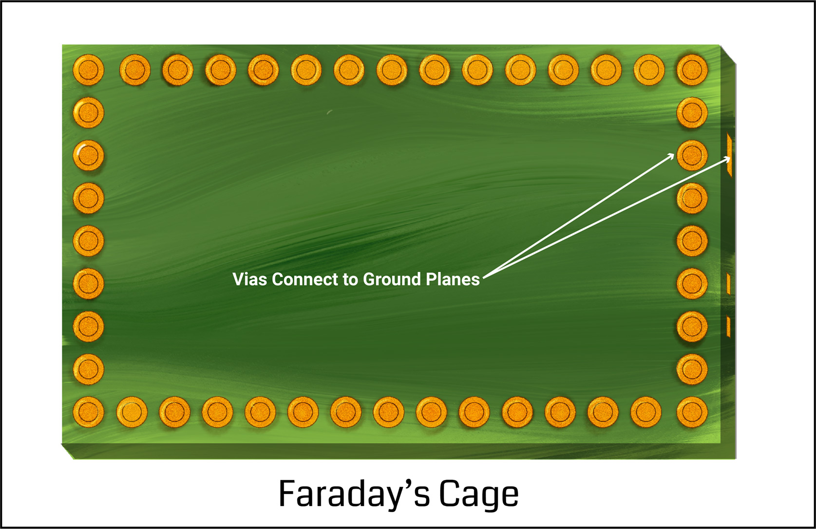
EMI and RF shielding is a method used to prevent electromagnetic and radio frequency interference from external signals. It also inhibits high-frequency signals from leaking out and interfering with surrounding circuits. This is achieved by using metallic barriers to absorb the electromagnetic interference that is being transmitted through the air. The shielding effect is based on a principle used in a Faraday cage, which states that the metallic screen completely surrounds either the sensitive or the transmitting electronics.
A Faraday cage is established by placing ground points on the edge of the circuit board. The goal is to avoid routing signals outside this area. This approach keeps EMI within the acceptable limit.
To learn about the basics of RF boards, see 7 factors that impact RF PCB design.
Flex shielding design challenges
You will come across a variety of design challenges when considering EMI shielding for flex boards. All shielding approaches increase the flex circuit thickness and cost to some extent. The most common difficulty is an increase in thickness which leads to a violation of the bend criteria. This raises concerns about mechanical failure and reliability. The additional expense might be substantial. Apart from this, the layer count of the design can go up.
Controlled impedance is the most frequent combination of shielding and other electrical needs. This increases the flex thickness even further, making it more difficult to fulfill both electrical and mechanical design criteria. There are a number of options to minimize both the absorption and/or the radiation of noise flexible PCBs. Some of them are discussed below.
To understand different types of failure like mechanical, environmental, thermal, etc., refer to 6 types of electronic component failures in PCBs.
Flex PCB shielding considerations
While selecting the type of EMI shielding for flex PCBs it is necessary to consider:
- Bend requirements
- Controlled impedance
Bend requirements
Each shielding approach contributes to the flexible circuit’s total thickness. Since the minimum bend capacity is a function of thickness, it will restrict or reduce a flex PCB’s bendability. As part of the design and material selection process, the minimum bend radius and bend type requirement for shielded designs must be precisely established and evaluated.
Additional restrictions are imposed by the type of bend required, whether static or dynamic. The bending capacity of a dynamic flex board is significantly greater than that of a static bend design.
To design better flex PCBs with Vern Solberg’s expert pre-layout tips, read flex PCB design guidelines part 1: pre-layout considerations.
Controlled impedance
The EMI and RF shielding approach is further limited by controlled impedance signal requirements in flexible PCBs. The shield(s) must have electrical properties that meet both EMI and reference plane criteria in order to obtain the appropriate regulated impedance values. Not all shielding techniques meet both the requirements.

What are the three types of EMI and RF shielding used in flex PCB?
EMI shielding for flex PCBs is done using three types of materials.
- Copper layers
- Silver ink
- Specialized shielding films
Each material should be selected based on shielding performance, influence on mechanical bend capabilities, and suitability for controlled impedance designs.
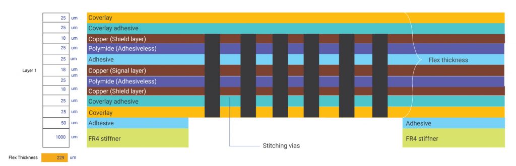
Copper layers
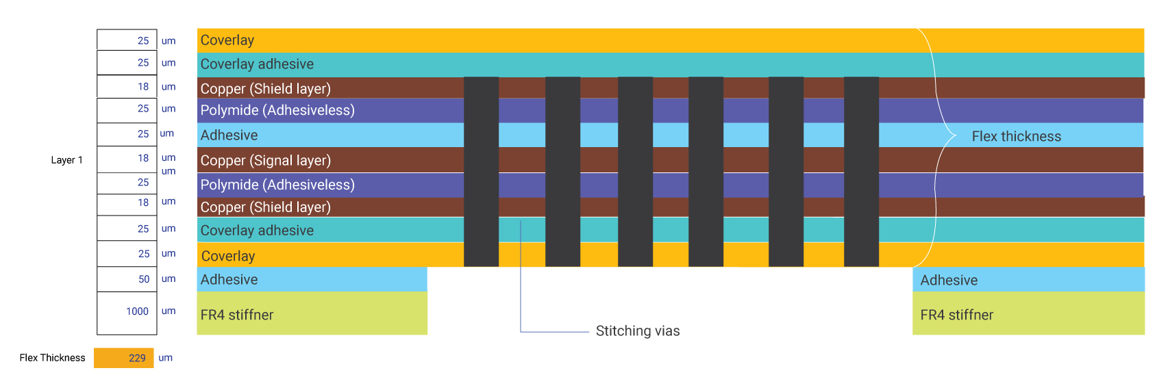
In this structure, the copper layers, either as solid or cross-hatched planes, are linked to the ground through stitched vias. The signal layers are sandwiched between the shield layers. This shielding solution is also utilized in rigid PCB design. Solid copper layer provides a higher degree of shielding. Cross-hatched layers are used if shielding is to be made without hampering the flexibility of the board.
While it is a very efficient shielding option, it has the disadvantage of raising the design thickness and part cost substantially. When the flex circuit is bent into its desired shape, the extra thickness limits the bending capability of the design, thus posing a reliability problem. A three-layer copper shielded flex circuit is almost 125% thicker than a single-layer non-shielded variant. This type of shielding supports controlled impedance design.
If the design has a single layer of circuitry to meet the connection requirements and requires shielding then the cost difference might be considerable. This particular design will be considered as a 3-layer board. Both the additional layers added for shielding will contribute to the overall expense.
Cross-hatching the copper shield layers improves the design’s flexibility, and may lower the effectiveness of shielding.
The shielding layers are connected to the ground plane through vias. This becomes a drawback due to the presence of vias in the flex area. According to IPC 2223, vias in the flex section are not recommended. They function as mechanical stress concentrators while reducing flexibility.

High-Speed PCB Design Guide
8 Chapters - 115 Pages - 150 Minute ReadWhat's Inside:
- Explanations of signal integrity issues
- Understanding transmission lines and controlled impedance
- Selection process of high-speed PCB materials
- High-speed layout guidelines
Download Now
Silver ink
Silver ink shield layers are a classic option. When compared to copper layers, silver ink offers the benefit of more flexibility and lower cost. Although the ink is more flexible than copper, it still requires an extra coverlay to encase and preserve the silver ink. This type of shielding is thinner and less expensive than copper layer shielding. A silver ink shielded flex circuit is only 75% thicker than a non-shielded variant. To learn about flex board cost optimization, see what are the cost drivers of flex PCBs.
Silver ink employs selected perforations in the main coverlay. These perforations expose the ground planes and allow for electrical interconnection. The silver ink flows into these holes and establishes a connection between the shield and ground/signal layer.
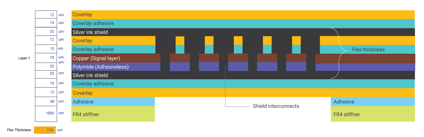
Silver ink is considerably inexpensive when compared to other EMI shielding materials. The number of material layers and manufacturing process steps are reduced in this case. For most controlled impedance designs, this is not a feasible option.
Specialized shielding films
Specialized shielding films are the most common option. They are suitable for dynamic bend applications and allow for the smallest possible structures. Shielding films are extremely effective and are used in a variety of sensitive applications.
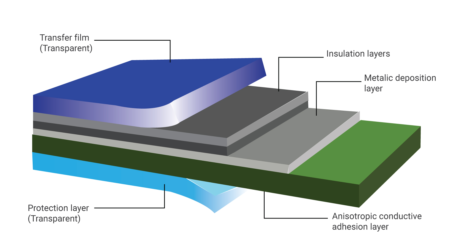
In this structure, an electrically conductive adhesive, a metallic deposition layer, and an exterior insulating layer are laminated together. It is then bonded onto the surface of the coverlay using heat and pressure. The ground circuit(s) are connected using the same way as silver ink. The conductive glue can bind and electrically link through selective holes in the coverlays.
The thickness impact is the smallest of the three methods. The thickness of a 2-sided shielded film is only 15-20% that of a non-shielded film.
This type of shielding is not recommended in controlled impedance designs as it increases the tolerance value.

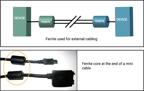
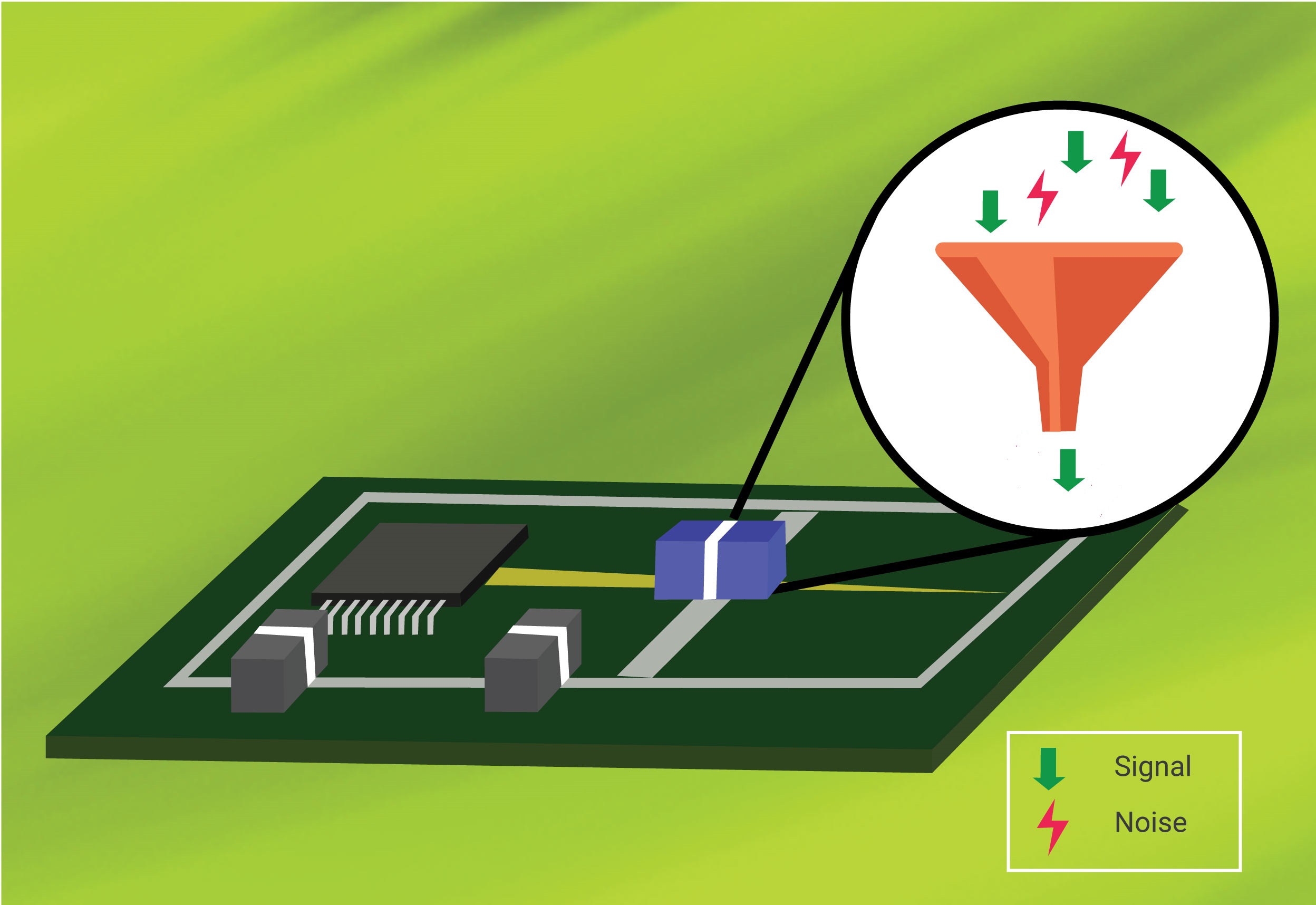
How do ferrite beads reduce EMI?
Ferrite beads are passive electronic components that can attenuate high-frequency signals on a power supply line. They are normally placed around a power line, such as the power cord of a laptop.
To learn the techniques of reducing signal attenuation in high-speed designs, see how to reduce signal attenuation in high-speed PCBs.
Ferrite beads act as inductors, which oppose changes in current. That means if a component is trying to draw a spike of current, the bead will resist that peak and can hinder the circuit’s operation. A bypass capacitor is needed to store up the charge that can provide power spikes. Ferrite beads block noise (unwanted rapid changing signal) and thus reduce EMI.
Design tips to avoid EM and RF interference in flex boards
- Sharp angles in the conductive traces result in fluctuating characteristic impedance and signal reflections. These sharp bends should be avoided using curved traces.
- Isolate high-speed and low-speed signals.
- Have the current return path as short as possible. This reduces the size of the current loop and therefore, radiation.
- Avoid placing vias in differential pairs as it leads to parasitic capacitance.
- If the design requires split ground planes, ensure that these ground planes are connected at a single point.
- Ground and power planes should be pulled back from the edge of the board.
- Implement the mSAP (semi-additive fabrication process) technique while designing RF circuit boards for 5G devices to avoid signal degradation and impedance discontinuity.
Shielding requirements are critical for any circuit board and flex PCBs are no exception. To provide a functional, dependable, and cost-effective shielding, a thorough examination of all electrical and mechanical design factors is necessary. Let us know in the comments section if you would like us to assist in reducing EMI in your board design. You can also read our design guide to learn about calculating bend radius and via specifications.
Flex PCB Design Guide
10 Chapters - 39 Pages - 45 Minute ReadWhat's Inside:
- Calculating the bend radius
- Annular ring and via specifications
- Build your flex stack-up
- Controlled impedance for flex
- The fab and drawing requirements
Download Now
About Milan Yogendrappa : Milan Y is an electronics and communication engineer with over 6 years of experience in developing and editing technical articles related to PCB design, manufacturing, and assembly. He is currently the editor-in-chief at Sierra Circuits.


