The selection of surface finish for a PCB plays a prominent role in circuit board assembly. Some of the most popular lead-free surface finishes include electroless nickel immersion gold (ENIG), ENEPIG (electroless nickel electroless palladium immersion gold), immersion silver (ImAg), immersion tin (ImSn), organic solderability preservative (OSP), and Pb-free HASL. These finishes influence assembly capability, PCB shelf life, solder joint quality, cost, and performance.
What is ENEPIG finish?
ENEPIG is a type of surface finish done on a copper layer to protect it from corrosion and oxidation in printed circuit boards. It is suitable for high-density SMT designs.
It is prepared by depositing electroless nickel (Ni 3-6 μm), followed by electroless palladium (Pd 0.05-0.15μm), and an immersion gold layer (Au 0.03-0.05 μm). It is ideal for solder joint strength, aluminum wire bonding, and gold wire bonding. ENEPIG is popularly known as a universal finish because it can easily be deposited on almost any PCB.
For controlled-impedance designs, ENEPIG is preferred at very high frequencies (≈40 GHz and above).
ENIG includes a relatively thick nickel layer, which has higher resistivity and increased skin-effect losses, leading to higher insertion loss at millimeter-wave frequencies.
At lower frequencies, the impact of the nickel layer is minimal, so both ENIG and ENEPIG perform similarly from an impedance standpoint, and either finish can be selected based on cost, availability, or assembly requirements.
Furthermore, it follows RoHS compliance. ENEPIG is an excellent finish for BGA substrates since it is both solderable and bondable.

Design for Manufacturing Handbook
11 Chapters - 96 Pages - 90 Minute ReadWhat's Inside:
- Annular rings: avoid drill breakouts
- Vias: optimize your design
- Trace width and space: follow the best practices
- Solder mask and silkscreen: get the must-knows
Download Now
Why ENEPIG?
- Offers low contact resistance: The electrical resistance is uniform, hence, easier to predict amperage.
- Follows RoHS compliance: Palladium completely dissolves into the solder, leaving an oxide-free nickel surface, which allows a reliable tin-nickel intermetallic.
- Black pads are not an issue with ENEPIG: Black pads are referred to as the dark, corroded, and oxidized Nickel. With the ENEPIG surface finish, it is no longer an issue.
During a webinar, one of the attendees asked:
“Which surface finish do you recommend for the best performance till 40 GHz?”
Steve Carney, R & D Project Manager at Sierra Circuits, replied:
“For best electrical performance up to 40 GHz, ENEPIG is recommended, as it minimizes nickel-related RF losses and provides excellent surface planarity and reliability for fine-pitch and high-frequency designs.”
For applications that require durable edge connectivity in addition to advanced surface finishes, learn how gold fingers enhance electrical reliability in connector-based designs.
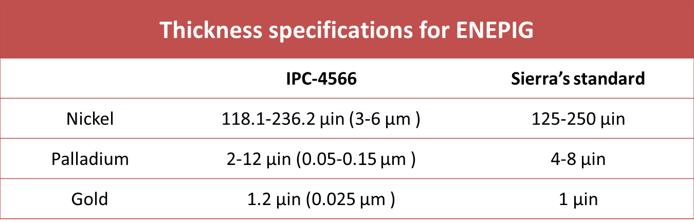
Thickness specifications
According to the IPC-4556 specification, the thickness of all the constituents in ENEPIG is clearly defined.
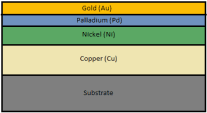
ENEPIG deposition process
ENEPIG consists of four layers of metal deposited on a board surface. These are copper, nickel, palladium, and gold. The process of creating this surface finish involves the following stages:
Copper activation
The copper layer that needs protection is selectively activated; this decides the deposition pattern in the electroless nickel plating stage. This process is done using a displacement reaction, which makes the copper layer serve as a catalytic surface.
Electroless nickel
Nickel prevents copper from reacting with the other metals used in the plating process, especially gold. The layer is plated on the catalytic copper surface using an oxidation-reduction reaction. This results in the formation of a thick layer (3-5 microns).
However, ENEPIG plating may not be the best choice for advanced PCBs with tight trace spacing. The EN layer in ENEPIG adds bulk to the trace edges, reducing clearance between conductors and increasing the risk of electrical shorts.
EPIG surface finish eliminates the electroless nickel layer, significantly reducing material build-up on traces and allowing for finer features and reduced clearances.
Electroless palladium
The palladium layer acts as a barrier layer between nickel and gold. This differentiates ENEPIG from the ENEG surface finish. Palladium prevents nickel from corroding and diffusing with gold. It also has anti-oxidant and anticorrosive properties. This palladium layer is deposited through an electroless reaction (oxidation-reduction). Thereafter, nickel reacts with palladium and forms a thin layer. This palladium is plated with a thickness of 0.05 to 0.1 microns, subject to application.
Immersion gold
Gold is the finishing layer that is applied in ENEPIG to provide benefits such as reduced contact, friction, and oxidation resistance. Gold maintains palladium’s solderability. Immersion gold plating uses a displacement reaction in which palladium dissolves and releases electrons, reducing gold atoms around it. Later, the gold ions attach to the surface of the circuit board, replacing some palladium ions. This results in a comparatively thin outer layer, ranging from 0.03 to 0.05 microns thick, considerably lower than any other solution using gold-plating methods.
Features of ENEPIG
The following chart shows the characteristics that define ENEPIG as the best surface finish:
- There is no possibility of grain boundary corrosion of the nickel surface by immersion gold.
- It withstands multiple lead-free reflow soldering cycles.
- It demonstrates excellent gold wire bondability.
- The process costs substantially less than electrolytic nickel gold or ENIG.
- The multiple electroless depositions of nickel, palladium, and gold metals help minimize porosity and protect the copper layer beneath them.
- While dealing with high-frequency circuits, nickel might interfere with and distort high-frequency signals. The palladium layer on top of nickel can negate the influence of nickel on high-frequency signals.
- In mixed technology, i.e., when RF and digital circuits are involved, opting for a direct gold surface finish will lead to assembly-related issues. Whereas ENEPIG is compatible with mixed technology and various assembly processes.


