Pads are the exposed copper areas on a PCB that provide connection points for components during soldering.
The two main pad types, solder mask-defined (SMD) and non-solder mask-defined (NSMD) pads, differ in how the solder mask overlaps or exposes the copper pad. This distinction impacts solder joint strength, manufacturability, and inspection outcomes.
The use of SMD or NSMD pads optimizes solder joint durability, structural stability, and manufacturing fabrication efficiency to suit component and layout constraints. SMD pads provide strong pad adhesion and minimize solder bridging, whereas NSMD pads maximize solder joint strength and electrical conductivity.
Here, you’ll learn when to use SMD and NSMD pads for reliability and manufacturability.
What are solder mask-defined pads?
SMD pads are copper features on PCBs where the solder mask partially overlaps the pad, leaving only a controlled area exposed for soldering. In this design, the pad size is determined by the solder resist opening.
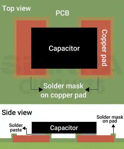
The overlapping solder resist restricts solder flow and improves the bond between the pad and the PCB substrate. SMD pads help prevent pad lifting, especially for larger components, and avoid solder spread for more controlled solder deposition.
However, the reduced copper area can impact electrical performance, and the board tends to concentrate stress at the solder joint, increasing the risk of failure during thermal cycling.
How do SMD pads improve solder paste transfer efficiency?
One of the reasons SMD pads are often favored for fine-pitch components such as BGAs and QFNs is their superior solder paste transfer consistency.
The solder mask overlaps the edges of the pad, forming a tight seal between the circuit board surface and the SMD stencil. This creates a well-defined cavity that guides the solder paste precisely during printing.
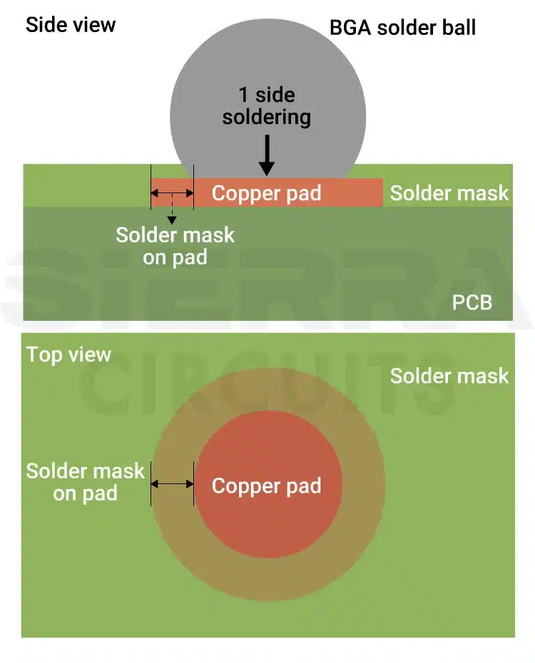
With identical stencil thickness, paste, and print settings, SMD pads yield higher and more consistent paste volumes than NSMD ones. This consistency is important because uneven paste deposits can lead to defects like solder bridging or weak solder joints.
What are non-solder mask-defined pads?
NSMD pads expose the entire copper pad by having the solder resist opening larger than the copper pad. The pad size is defined by the copper feature rather than the solder mask.
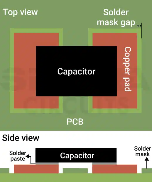
NSMD pads provide stronger solder joints, as the solder wets all sides of the land pattern (as shown in the above image). This leads to better solder fillet formation and improved stress distribution. In addition, they offer greater flexibility for trace routing and make repairs easier.
However, NSMD pads have less mechanical strength since the solder joint depends solely on copper adhesion, increasing the risk of pad lifting, especially with larger BGA components. These pads are preferred when solder joint reliability and electrical performance are prioritized over mechanical robustness.
How NSMD pads improve solder bonding and reduce defects
While NSMD pads are more prone to variation in solder paste transfer due to less effective stencil gasketing, they offer a larger exposed copper area for solder wetting. The solder flows over both the top and side walls of the pad, forming stronger intermetallic bonds.
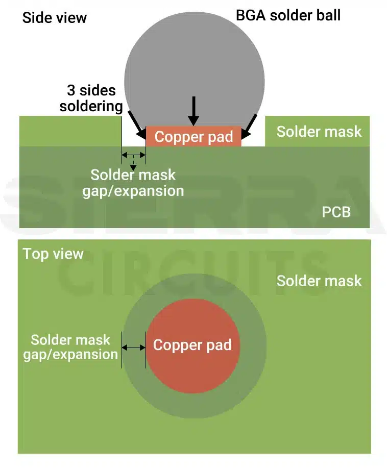
This extended wetting improves joint reliability by distributing thermal and mechanical stresses evenly. As a result, NSMD pads are often preferred for solder joint integrity, especially in applications with high thermal cycling demands.
Additionally, NSMD pads reduce the risk of random solder balls caused by stencil misalignment. If paste is deposited slightly off-center on a mask-defined pad, some may land on the solder mask (which won’t bond), leading to isolated solder balls. NSMD pads, by contrast, leave more margin for alignment error.
Download our eBook to learn more about design for assembly.

Design for Assembly Handbook
6 Chapters - 50 Pages - 70 Minute ReadWhat's Inside:
- Recommended layout for components
- Common PCB assembly defects
- Factors that impact the cost of the PCB assembly, including:
- Component packages
- Board assembly volumes
Download Now
When to implement SMD and NSMD in your PCB layout
Selecting the appropriate pad type is crucial for ensuring reliable solder joints, mechanical stability, and manufacturability in your circuit design.
| Use cases | How SMD pads help |
|---|---|
| Fine-pitch components | The solder resist overlapping the pad reduces the risk of solder bridging and ensures reliable connections. |
| Limited board space (HDI layouts) | SMD pads allow for smaller exposed areas, minimizing the risk of short circuits in compact layouts. |
| Precise solder paste control | The solder mask opening acts as a gasket, improving paste distribution and reducing overflow. Ideal for high-speed SMT lines. |
| Automated reflow assembly | SMD pads are well-suited for automated processes, as they offer high alignment accuracy. |
| Mechanical reinforcement | In applications involving stress (e.g., automotive, aerospace), the solder resist overlap provides stronger pad anchoring, reducing the risk of pad lifting. |
| Use cases | How NSMD pads help |
|---|---|
| Standard-pitch or hand-soldered components | Larger pad areas accommodate soldering iron tips better, making NSMD ideal for prototyping or manual assembly. |
| Looser fabrication tolerances | NSMD pads are less affected by solder mask misalignment due to larger mask openings around the pad. |
| Enhanced solder wettability | More exposed copper improves solder flow and joint formation. |
| Stronger solder joints | NSMD pads allow solder to flow around the entire copper area, forming more reliable joints under thermal cycling conditions. |
Fabrication notes for SMD and NSMD pads
- Pad definition: All pad designs must conform to the component manufacturer’s recommended land pattern specifications.
- Solder mask and copper tolerances: Ensure solder resist alignment and copper etching tolerances meet IPC-7351 guidelines.
- Pad type specification: Specify whether each pad is SMD or NSMD. Highlight critical components (e.g., BGAs, QFNs) that require SMD pads for alignment precision.
- Example: Components labeled C1, C2, and others use solder mask-defined pads. Do not modify the solder resist for these parts.
- Vias under SMD pads: All vias placed under SMD pads must be filled and planarized to prevent solder wicking during reflow.
- NSMD pad exposure: Ensure full copper exposure for NSMD pads; no solder resist should overlap the pad edges.
- Stencil alignment: The stencil aperture must match the solder mask opening to enable consistent solder paste deposition within the defined pad area.
- Via structures: Use via-in-pad (VIP) with filled/plugged vias for SMD pads. For NSMD pads, use dogbone via structures where applicable to prevent solder joint disruption.
- Copper etch tolerance: Maintain tight copper etching tolerances (±0.5 mil or better) to preserve accurate pad geometry.
To learn flux selection and application techniques, download our soldering flux eBook.

Soldering Flux eBook
13 Chapters - 24 Pages - 40 Minute ReadWhat's Inside:
- Why flux is needed
- The ingredients of flux and what they do
- Soldering flux categories
- How to read a flux manufacturer’s technical data
- The best flux for various applications
Download Now
SMD Vs. NSMD pads in PCBs
Always prioritize component datasheets and your circuit board fabricator’s specific capabilities to ensure all designs are manufacturable and reliable.
| Design aspect | Solder mask-defined pads | Non-solder mask-defined pads |
|---|---|---|
| Pad dimensions | 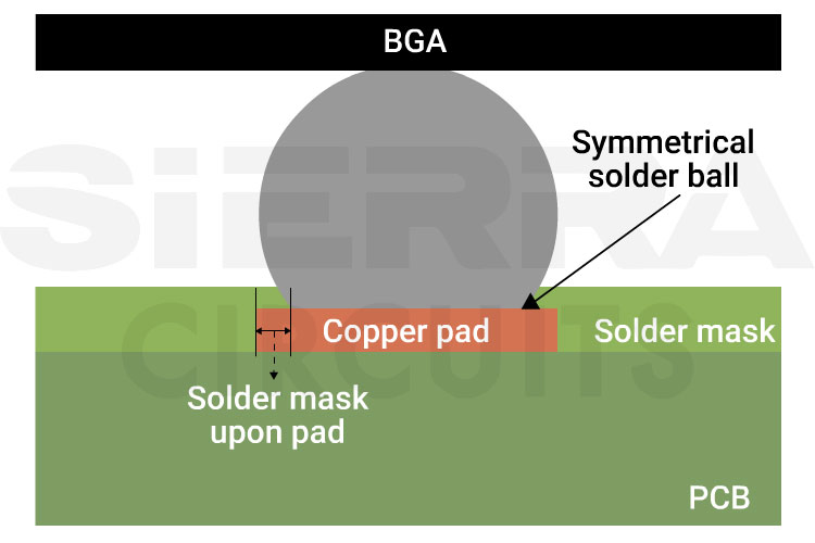
Solder mask opening is smaller than the copper pad (typically by 1–2 mil). For BGAs, the copper pad diameter typically matches the BGA ball. |
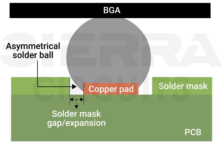
Solder mask opening is larger than the copper pad (typically by 1–3 mil). For BGAs, the copper pad diameter is ~20% smaller than the BGA ball. |
| Customized pad shapes | Limited support for custom shapes |
Supports custom shapes like dogbone or dumbbell pads |
| Typical solder mask web (solder dams) | 1-3 mil | 3–10 mil |
| Copper-to-copper spacing | Less critical; solder mask acts as a dam. Routing is more constrained in tight BGA layouts. | Requires more spacing; the mask does not cover the copper edges. Offers more routing space between pads, beneficial for high-density BGAs. |
| Via structures | Via-in-pad (VIP) | Dogbone and VIP |
| Thermal relief and mechanical performance | Not required; a full copper connection improves heat dissipation. Better mechanical anchoring, suited for heavy or large BGAs (e.g., in automotive/aerospace). | Often needs thermal relief to aid soldering. Less mechanical strength, higher pad lift risk for large BGAs. |
| Soldering process | Solder is restricted to the mask opening, aiding alignment during reflow. | Solder wets the top and sides of the pad, forming stronger joints. Requires precise stencil control to prevent solder overflow. |
| Solder voiding risk | High | Low |
| Layer registration | Requires precise alignment of the solder mask to the pad to ensure correct pad exposure. | Less sensitive to mask-to-pad alignment since the copper defines the pad boundary. |
| Assembly methods |
Well-suited for automated pick-and-place assembly. Manual soldering is more difficult. Offers better pad adhesion during rework. |
Suitable for manual soldering and rework. The pad may be more susceptible to lifting if not handled carefully. |
Sierra Circuits ensures precise SMD and NSMD pad design and fabrication with advanced printed circuit board manufacturing. See our rigid PCB manufacturing capabilities to learn more.
5 common design mistakes in SMD and NSMD pads and how to avoid them
When implementing SMD or NSMD pads, you must avoid the following common design mistakes that can compromise PCB reliability or manufacturability.
| Design challenge | Description | Solution |
|---|---|---|
| Inconsistent pad geometry and sizing | Uneven pad shapes or mismatched sizes can cause tombstoning during reflow. | Keep pad shapes symmetrical and maintain consistent sizes across terminals to ensure balanced solder flow and stable PCBA. |
| Inaccurate solder mask layer alignment | For SMD pads, inaccurate solder mask registration can expose unintended copper, distort pad shape, or cause shorting. | Confirm your fabricator’s alignment tolerances and size solder mask openings accordingly to ensure proper pad exposure. |
| Improper via placement near pads | Placing vias too close to pads, especially without proper via filling or via tenting, can cause solder wicking during reflow. This depletes solder from the joint and weakens mechanical integrity. | Follow manufacturer-recommended via-to-pad clearances, or use via-in-pad with filled and capped vias when space constraints exist. |
| Inadequate solder mask webbing between pads | Insufficient solder mask webs can break during fabrication, leading to solder bridging or mask delamination. This is particularly problematic in high-density layouts with fine-pitch components. | Maintain a minimum solder mask web width of 3 mil or more between adjacent openings. |
| Ignoring copper etching tolerances | Ignoring copper etch tolerances during pad design can result in undersized or misshaped pads, which compromise solder joint quality and component alignment. | Include copper etch tolerance margins (typically ±0.5 mil) in pad and trace designs, and confirm these tolerances with your circuit board fabricator upfront. |
For more on pad design, see what is a pad in PCB design and development.
Choosing between SMD and NSMD pads comes down to what your design needs. Use NSMD pads when you want better solder joints and easier inspection. Opt for SMD pads when you need stronger mechanical support, especially in tight spaces.
By understanding your component layout, manufacturing limits, and how the board will be assembled, you can make the right choice for a reliable and effective PCB.
