Conductive anodic filament (CAF) in aerospace and defense PCBs is an electrochemical failure in which copper filaments grow inside the laminate between two electrically biased conductors.
Circuit board designers should select high resin content materials and follow IPC-2221 creepage and clearance calculations to reduce the risk of CAF.
In this article, you will learn what causes conductive filament growth in printed boards and how layout engineers can reduce its occurrence.
Highlights:
- Fine glass weaves and spread glass laminates improve resin distribution around glass fibers and enhance CAF resistance.
- Controlled etch back and drilling processes help preserve hole-wall integrity and reduce copper migration pathways.
- Resin starvation, measling, and poor lamination control can lead to CAF growth.
Why is CAF critical in aerospace PCBs?
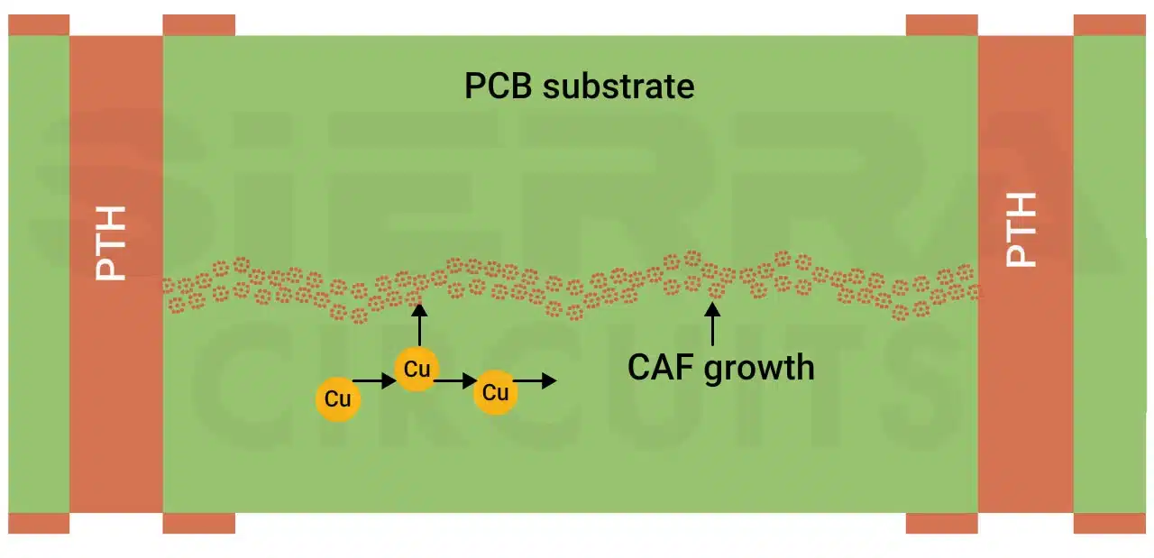
Conductive anodic filament is a major reliability concern in aerospace boards because it can create internal short circuits that lead to intermittent failures, signal leakage, or complete system breakdown in mission-critical electronics.
These prototypes are more prone to filament formation because they operate in harsh environments with high humidity, vibration, pressure variations, and continuous electrical stress. These conditions accelerate the electrochemical migration of copper ions inside the laminate and cause CAF growth.
What causes conductive anodic filament in circuit boards?
CAF in aerospace PCBs develops when moisture penetrates the substrate between electrically biased conductors. The risk becomes higher when resin bonding is weak, conductor spacing is too tight, resin fill in vias is insufficient, or the PCB is exposed to contamination, humidity, and temperature cycling.
The infographic below highlights the key factors that contribute to CAF formation in printed boards.
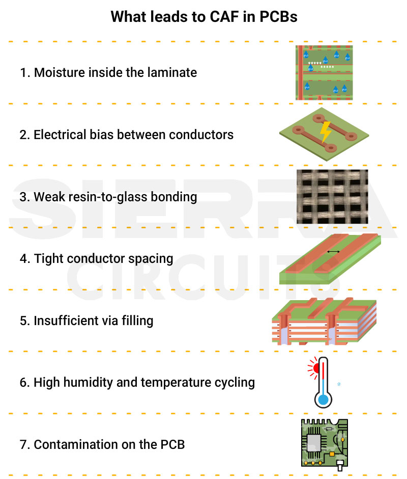
You can significantly reduce the risk of filament formation by making the right design and material selection decisions early in the layout stage. In the next section, we will cover how to prevent CAF in aerospace and defense boards.
How can designers prevent CAF growth in aerospace and defense PCBs?
Preventing filament formation requires proper material selection, adequate conductor spacing, and well-defined fabrication requirements. The following design practices help improve insulation reliability in IPC class 3 boards.
1. Use high resin content laminates with finer glass weave styles
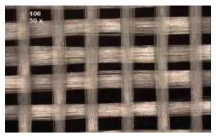
CAF resistance in circuit boards mainly depends on the glass structure and the resin content. Heavier glass weaves expose large glass bundles, which increases the possibility of copper migration along the fibers.
High resin content laminates help improve insulation by providing better resin coverage around the glass fibers. This reduces voids and weak regions where conductive anodic filaments can develop.
Select laminates with finer glass weave styles, such as 106 and 1080, and spread glass variants like 1067 and 1086. These materials help keep the glass fibers properly sealed within the resin system and reduce conductive path formation inside the substrate.
Spread glass structures offer better anodic filament resistance because they distribute the resin more evenly around the glass fibers.
High-performance materials such as Taconic, Rogers, and Panasonic Megtron laminates are commonly used in high-reliability aerospace designs due to their improved CAF resistance.
The table below lists some commonly used laminates with high conductive filament resistance and low moisture absorption properties.
| Manufacturer | Laminates | Moisture absorption (%) |
|---|---|---|
| Panasonic | Megtron4 (R-5725) | 0.14 |
| Rogers | RO4350 B | 0.06 |
| Taconic | CER-10 | 0.02 |
Sierra Circuits manufactures aerospace and defense circuit boards that meet stringent military and IPC class 3 requirements.
Our capabilities include:
- MIL-PRF-31032 compliant fabrication
- IPC class 3 FS builds
- Extensive electrical testing and inspection reports
- ITAR-registered and AS9100D-certified manufacturing
To talk to a PCB expert: Book a meeting with us or call us at +1(800) 763-7503.
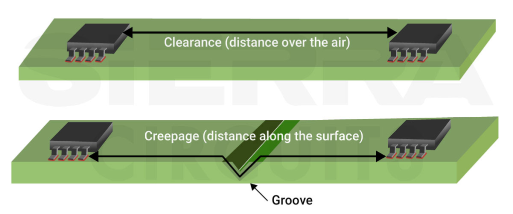
2. Follow IPC-2221 guidelines for creepage and clearance spacing
Insufficient spacing between conductive features increases the electric field intensity inside the laminate, increasing the risk of CAF in aerospace PCBs.
Maintaining adequate creepage and clearance as per the IPC-2221 standard can reduce electrical stress between adjacent conductors and avoid electrochemical conditions that promote copper ion migration inside the substrate.
3. Perform a DFM analysis before fabrication
Filament-related issues such as tight spacing, improper via placement, and stack-up pitfalls are not always easy to identify during layout development. Running a detailed DFM analysis helps detect these risks early.
Some common DFM issues that can increase CAF susceptibility include:
- Insufficient spacing between vias and traces
- Closely spaced through-holes under high voltage bias
- Inadequate dielectric spacing in the build-up
- Inadequate drill-to-copper clearances
At Sierra Circuits, we perform thorough DFM checks on spacing, build-up, and via structures before fabrication begins. This helps us identify potential risks and deliver high-quality, CAF-resistant circuit boards.
To learn more, visit aerospace and defense PCB manufacturing capabilities.
4. Ensure your fabricator maintains a minimum positive etch back
Positive etch back helps improve plating wraparound around inner-layer interconnects and supports better Z-axis reliability. However, excessive plasma etch back can increase CAF risk.
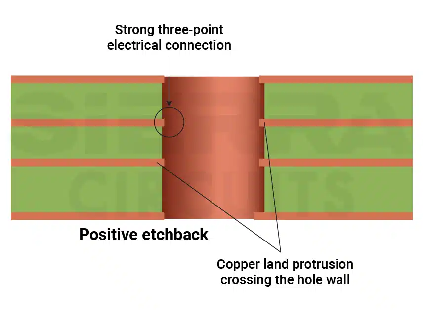
During plasma etch back, epoxy resin is removed while the glass fibers remain exposed. If too much resin is removed, the exposed fibers become vulnerable to copper migration and conductive filament growth.
Ask your fabricator to:
- Keep etch back requirements as low as possible (values range from 0.4 to 0.8 mil).
- Maintain adequate resin coverage around glass fibers.
You can mention the above requirements in your PCB fabrication notes.
5. Ask your CM to minimize glass-resin interface damage during drilling
Drilling quality plays a major role in CAF resistance in multilayer printed boards. During through-hole drilling, mechanical stress can develop at the glass-to-resin interface inside the laminate. This stress can create microscopic separation paths where conductive filaments later grow between adjacent vias or between a via and a trace.
Poor drilling can damage the hole wall, remove resin around the glass fibers, and expose the weave structure to conductive chemistry. As a result, copper migration takes place inside the laminate.
Specify the pointers below in your fab notes:
- Minimize drilling-related damage to the hole wall.
- Maintain proper resin coverage around glass fibers.
- Control resin flow and squeeze-out during lamination.
- Use controlled cure profiles during pressing.
- Inspect for resin starvation, measling, and delamination defects.
At Sierra Circuits, we optimize drill parameters, monitor resin flow during lamination, and control cure profiles to minimize glass-resin interface damage and reduce CAF risk in aerospace and defense PCBs.
Conductive anodic filament develops due to improper material selection and poor layout planning. By selecting filament-resistant materials, maintaining adequate conductor spacing, controlling via structures, and validating the design through DFM analysis, designers can reduce CAF in aerospace PCBs.
For conductor spacing guidelines, download the Trace and Space Handbook.

PCB Trace and Space Handbook
8 Chapters - 34 Pages - 40 Minute ReadWhat's Inside:
- Key factors influencing line width and spacing
- Clearance guidelines for high-voltage and high-speed traces
- DFM rules for heavy copper PCBs
- Via considerations
- Industry standards for trace and space design